background image

4.  B LOCK  DIAGRAM  AN D  N EW  CIRCUIT  DESCRIPTION 

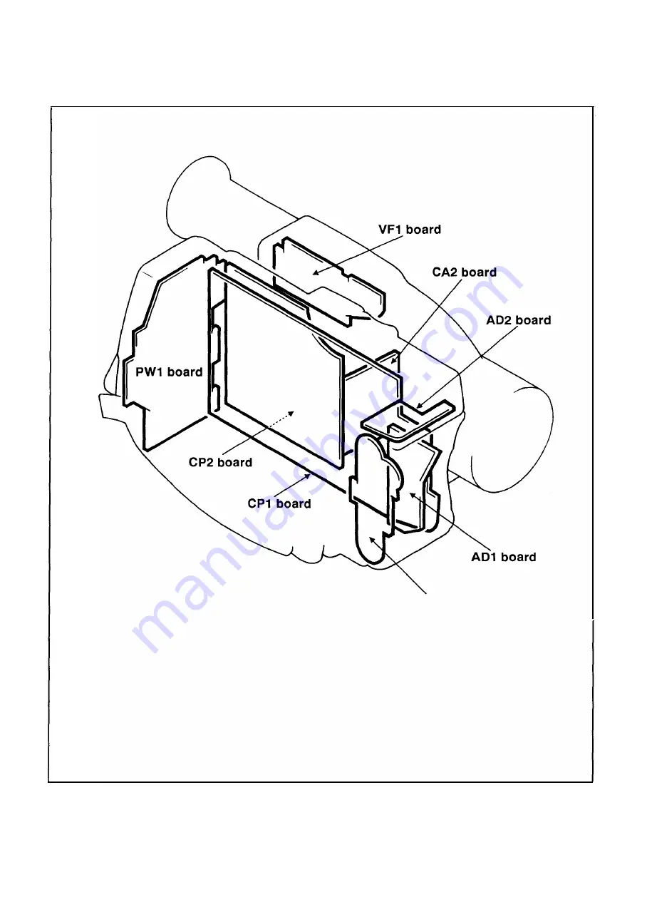
4-1 .  BOARD LOCATION 

AD1  BOARD:  AUDIO CIRCUIT 

AD2 BOARD:  MICROPHONE CIRCUIT 

CA2 BOARD:  CCD IMAGE CIRCUIT 

CP1  BOARD:  SERVO/SYSTEM CONTROL CIRCUIT 

VIDEO CIRCUIT 

CP2 BOARD:  CAMERA CIRCUIT 

PW1  BOARD:  POWER CIRCUIT 

TB2 BOARD:  TERMINAL CIRCUIT 

VF1  BOARD:  VIEWFINDER CIRCUIT 

- 4-1  -

TB2  board 

Содержание 126 032 00

Страница 1: ... 8 mm Camcorder VM EX70P EUROPE AUSTRALIA NEW ZEALAND Subject illumination 3 1 00 000 lux range Recommended 300 lux or more aubject illumination Power aupply 6 V battery pack 6 5 V AC adaptor charger Power conaumptlon 6 4 Wduring camera recording Operating o C 40 C 32 F 104 F temperature range Storage temperature 20 C 60 C range 4 F 140 F Dimenaiona W x H x 0 Weight Microphone Video output termina...

Страница 2: ...ls Model Name Reference No Parts List and VM EX70P PL 550010 Circuit Diagram RS MECHANISM MM 550005 Mechanism Manual RS MECHANISM MS 550001 Revision I AC Adaptor charger VAR S15 SM 550008 Service Manual LCD Color Monitor Remote Controller VRM 30P 30 SM 550009 Service Manual ...

Страница 3: ...OCK 6 3 VIDEO CIRCUIT 6 1 0 ASSEMBLY AND STAND ASSEMBLY 3_5 6 4 AUDIO CIRCUIT 6 1 3 3 7 REMOVAL O F CP1 BOARD AND 6 5 VIEWFINDER CIRCUIT 6 1 4 MECHANISM ASSEMBLY 3 7 7 VOLTAGE CHART 7 1 3 8 REMOVAL OF CAMERA LENS BLOCK 7 1 CAMERA CIRCUIT 7 1 CP2 BOARD AND MICROPHONE UNIT 3 8 7 2 SERVO SYSTEM CONTROL CIRCUIT 7 3 4 BLOCK DIAGRAM AND CIRCUIT 7 3 VIDEO CIRCUIT 7 7 DESCRIPTION 4 1 7 4 AUDIO CIRCUIT 7 1...

Страница 4: ... Ground H H HORIZ HD HHK HHS HPF l 1 0 I ID INT REC INS INV IR IRIS DET J JOG L LI LIM LP LPF M ME MECHA MF MIC MOA MON MP N NC NT O OS osc OSD P PB PG DOUB PI PLL PS PWM R REC REG REV REW S S S S REEL SCK SI so SP STB STBY SW T T TELE T E LED T REEL TC TP TSB Horizontal Horizontal Drive Half Horizontal Killer Half Horizontal Shift High pass Filter In Out Current Identity Interval Record Insert In...

Страница 5: ...C108 TL 7L XN1113 TW Note The codes of digital transistors show only the transistor numbers Identification With Two Letters Use this code and the chart for component identification Letter B Example Code BR Transistor Number 2SB1218A Number 2SB1218A R fil T L_Rank of DC Current Gain hFE Transistor Number Identification With One Letter and One Numeral Use this code and the chart for component identi...

Страница 6: ...less diodes are indicated by a code on the surface using one letter and one numeral one letter two letters two letters and one numeral or three numerals Code Diode Number Code Diode Number B SB05 05 CP TB MN MA141WA TX N DAN202U T106 MT MA141WK TX A2 DSH015 TL NP MA143A TX A4 DCF015 TL M3H MA721WA TX A6 DCG015 TL W6 DCGOlO TL C3 1SS302 TE85L 822 RD8 2M T1BB2 MH MA141K TX 8 2A MA3082 M TW M3H Schot...

Страница 7: ...0 µH ITJ ITJ L Tolerance J 5 K 10 Multiplier 0 1 2nd Significant Digit 0 9 Ist Significant Digit 0 9 Leadless Tantalum 1 Capacitance code Multiplier Capacitance code Value CD Working Voltage code __ _ _ _ Polarity Bar side CD W Y code Code G J A c D E Working 4 6 3 10 16 20 25 Voltage V Capacitance code Value Code A E J N s w Value I 1 5 2 2 3 3 4 7 6 8 Capacitance code Multiplier Code 5 6 7 Examp...

Страница 8: ...chanical stress and rubbing of the component electrode must be avoided 2 Removing leadless components Grasp the leadless component body with tweezers and alternately apply heat to both electrodes When the solder on both electrodes is melted remove the leadless component with a twisting motion Note a Do not attempt to lift the component off the board until the component is completely disconnected f...

Страница 9: ...2 x 6 p 2 x 5 Bp 2 x 12 p 2 x 4 Pp 2 x 3 p 1 4 x 2 5 Ps 1 4 x 3 p 2 x 4 Ps 1 4 x 1 6 Ps 1 4 x 2 2 Ps 1 4 x 3 Pp 1 4 x 2 Pp 1 4 x 3 5 1 4 x 2 1 4 x 3 p 2 x 5 p 1 4 x 3 Pp 2 x 4 Pp 2 x 6 Pp 1 6 x 3 5 p 1 6 x 4 5 Abbreviation Name Shape No symbol Special type D p Pan head D B Binding head Abbreviation Name Shape No symbol Machine screw I s Forming tight for metal J 0 p Forming tight for plastic J 0 b...

Страница 10: ...upward pull the top lid toward you to remove it To install the top lid place it on top of the mechanism assembly and then slide it away from you while pressing it down until it clicks into place If the power supply is interrupted because of a blown fuse the cassette holder will not open In this case first remove the cassette lid and then remove the top lid Cassette holder Connect the AC adaptor ch...

Страница 11: ...te holder and then lower the mechanism assembly Because the upper section of the mechanism is extremely delicate do not apply excessiveforce at this time 2 Remove the two screws and then remove the cassette lid CD 3 Remove the terminal cover Mechanism assembly CD Cassette lid Terminal cover 3 3 ...

Страница 12: ...gage the hook Then remove the front cabinet from the front of the camcorder _ o ll l i r 11111111111111111 Front cabinet i I I I I I I I I Lens section I Screw 1 7 x 6 104 i The two connectors for the microphone and for the accessory shoe should be disconnected at this time also 3 Remove the five screws J and and then remove the cabinet assembly right J Screw 2 x 5 99 1 Screw 1 7 x 4 101 i J Screw...

Страница 13: ...en remove the view finder block assembly from the cabinet assembly left 3 Pull out the eye piece fully and then push it back slightly Turn it toward the left in the direction of the arrow and then remove it 4 Remove the screw and then remove the cabinets right and left of the viewfinder 5 Disconnect the two connectors and to separate the viewfinder board section Viewfinder block assembly J________...

Страница 14: ... three screws and then while pushing the hooks remove the camera block assembly from the VTR block assembly PW1 board l Hooks 3 Remove the two screws and then remove the stand assembly When carrying out the steps in 5 ELECTRICAL AD JUSTMENT remove the camera block assembly but not the PW1 board Stand assembly i v Screws 1 7 x 6 1 04 Screws 1 7 x 4 1 00 3 6 ...

Страница 15: ... condition the CP1 board can be turned 1 80 3 Disconnect the four FPCs and J disconnect the two ground lead wires and which are soldered to the shield case of the CP1 board and then remove the CP1 board from the mechanism assembly 4 Remove the screw and then remove the AD1 board from the terminal bracket 5 Remove the five screws and then remove the two brackets and the terminal bracket from the me...

Страница 16: ...the screw and then remove the microphone holder and two microphones AD2 board and microphone pad Note For detailed information on how to remove the components please refer to the Parts List manual 3 Remove the two screws J and then remove the acces sory shoe from the front cabinet Microphone holder Microphones l Screw 2 x 5 99 esso shoe _ AD2 bo d Microphone holder 0 Microphone pad Front cabinet F...

Страница 17: ...CATION AD1 BOARD AUDIO CIRCUIT AD2 BOARD MICROPHONE CIRCUIT CA2 BOARD CCD IMAGE CIRCUIT CP1 BOARD SERVO SYSTEM CONTROL CIRCUIT VIDEO CIRCUIT CP2 BOARD CAMERA CIRCUIT PW1 BOARD POWER CIRCUIT TB2 BOARD TERMINAL CIRCUIT VF1 BOARD VIEWFINDER CIRCUIT 4 1 TB2 board ...

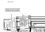
Страница 18: ... I I I I VIEWFINDER 1 VF 1 BOARD I G G G H H 1 2 3 K ocu s H DRIVE H D EF I U F B T C R T v srzE I H V I _J DY IC971 BA7149F i I iii m E r T1 0 z 0 c m c 0 m C r 0 Video g s 5V c GND C 0 s ...

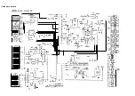
Страница 19: ...2 CAMERA BLOCK DIAGRAM CAMERA BLOCK CA2 CCD MAGER BLOCK IC951 ICX059AK I 15V _j_ Jt A PG DIAGRAM IC914 CXAl391R 110 111 108 ...

Страница 20: ...9 T SYNC __ B I CAMERA FEATURE 109 1117 TQT OAT TO CPD CN933 CTC A BLOCK TO CPD CN933 SCK l so 2 CAM CS 16 CP2 1 cr l cQNVERTER 2 MC145053 1rcm rJ1l II I C936 I LA6358NM I HALL DRIVEj I 1 I I 1 I ZOOM I I ENCffiDER CN93l 14 j E PROM I I I IRIS 1 I ...

Страница 21: ... 1 J CAM ADJ IRIS 18 CAM ADJ2 9 A fZ DET 16 CAH ADJ3 1 TO PWD CN911 8 SV t NEG 3 SVCS 4 SV 5 5YCl1 6 GNl 7 GNl PG IC914 4 3 112 109 JC913 CXL15i7N IC914 CXA1391R IC9 9 CXL5504 CAMERA SIGNAL PROCESS CVC A ...

Страница 22: ... AMERA SIGNAL PROCESS CVC A BLOCK CTO CPD CN933 1 c CAMERA FEATURE CTC A BLOCK IC931 STANDARD CELL LC97000A 376N IC932 MICRO PROCESSOR S87C51FC 1 IC936 LA6358NM 1 tt HALL DRIV LENS BUICK ...

Страница 23: ... DATA 0 i l CG REC BLNK 1 CG DISP DATA u OS DISP BLNK J OS DISP DATA 0 _j IC341 ANO BATE J 4 IC345 SYNC SEPARATOR JOG VDD 4 JOG H U IE LCD JOG H D 4 1 RtCCRA u IEC 1 REC CHBD 4 ll FEP A MUTE D 4 I V MUTE o IEC 1 SP LP RFSW P8 0 1 HIB DET QUT U 1 CIM SYNC HIS OUT HIBlEMP LP SEPA REC SCK TALLY LED REMOCON ON LCD ON LCD JOG H REC CHA REC CHB FEP A MUTE V MUTE SP D5 RB_Wi PB SIG DET HI8 DET OUT COMP S...

Страница 24: ...UT COMP SYNC HI8 OUT HI8 MP LP SEPA REC SCK VIDEO CENTER ADJ IC352 BATTERY BACK UP VOLTAGE REG IC381 ORl fu filf R Q350l MP 5V CN321 LITHIUM BATTERY MECHANISM BLOCK CN334 CCN338l J3801 LOADING MOTOR MODE SW DEW SENSOR SUPPLY REEL SENSOR TAKEUP REEL SENSOR TAPE TOP END SENSOR RECOGNITION SW CASSETTE IN SW CAPSTAN MOTOR CAPSTAN SENSOR ...

Страница 25: ..._ 0 1 _T c E LE J li F i F lj p pAL t 4 SCAN IN 5 SIN 6 EJECT SCREEN EDIT WIDE F SCAN IN 6 t s c rN 7 L c o _ N _ G l ll l n t E D I Tc i fo 11 4 15 SCAN IN 7 SCAN OUT 4 SCAN OUT 3 _ SCAN OUT 2 mrr5 0 il t t _ _ SCAN OUT 1 VlJCS SCAN OUT 0 f CAM CS J I IC371 12 11 14 ATF 111 u 1 1 PR IC353 Cl 4l POWER SAVE PB PILOT 2 BPF BM PB RF n 1 I o rli c c m I 616 REC PILOT S IQ3701 REC PILOTn 1_ 1 5 l ANSr ...

Страница 26: ...P4616 TSB 1rc t bJ SEL 2 SEL 1 ATF ERROR DRUM PG DRUM FG CLKO CLK1 CAM ON MC PWM MH PWM VTR ON Q3301 Q3302 IC361 CAPSJ fvffTOR IC381 ORl fu filf R S S SV VF 5V VA SV UNREG SCAN IN 1 SCAN IN 0 SCAN IN 2 SCAN IN 3 SCAN OUT 3 A3001 OC OC CONVERTER STANBY H OLD VTR BLOCK READY VTR CAPSTAN MOTOR CAPSTAN SENSOR DRUM MOTOR S R ER307_BLOCK DRUM VS CAP VS UNREG POWER MOTOR DRIVE BLOCK CAM CAM ON CAMERA BLO...

Страница 27: ... S S 5V TEST NOT USED 15 NOT USED 16 NOT USED 17 NOT USED 18 NOT USED 19 NOT USED 20 AUDIO L IN AUDIO R IN CH A X CH A Y GND CH B X CH B Y GND GND GND GND FE X FE n 4 5 Lal VIDEO H18 1 Rl75 1Rl76 IC101 CXA1207AR F CAIERA 5CK 1f CAIERA CS IHEG l HEG GND SYNCRO EDIT LCD VDD LI 50 PCl1ER SAVE FADE V l UTE A l UTE PB RF T p REC PILOT CCJf SYNC JOG VD SEPA REC SPIO JOG H l f AE CG REC DATA CG REC BUN C...

Страница 28: ...B2 BOARD IC291 LA7471M p STEREO MATRIX p R NR CIRCUIT R _i _ R 1 5MHZ MOD 1 7MHZ MOD tR p 1 5MHZ _ ____ DEMOD 1 7MHZ DEMOD 1 SMHZ BPF 1 7MHZ BPF AUDIO L OUT 011 1 S P LP AUDIO R OUT LCD AUDIO IC201 LA7492W SP LP L 1 1 FADE L 1 PB REC CAM LINE L l 1 A MUTE LINE ON 4 6 ADJ DEV ADJ cu DEV ADJ CR REC A PB RF FROM SISCON ...

Страница 29: ...CS 12 FS 5V 13 cs 14 SK 15 DO 16 DI 17 FSGND 18 A 19 I I Zoom position sensor I I I I I II I I I I I I I I I I I I I iI I I I I I Iris motor 7 6 5 I 2 3 4 I I I Aut _ o 1 eria switch I II I L r 1 Lfi_ T T 1 1 B 20 I I E PROM Auto focus Zoom motor I A 21 I B 22 I I I ZOOM 23 _I ZOOM 24 I CN932 vcc 1 MF1 2 1 T __ i 1 MF2 3 1 t __ 1 1 1 GND 4 motor _J L 1 4 7 ...

Страница 30: ...cording Two built in omnidirectional microphones record the sound with an abundant feeling of ambience 7 Auto Date The Auto Date function is constantly powered by a lithium battery Once the date is set it is automatically incre mented 8 High Speed Shutter Even when a fast moving subject is recorded slow or still pictures do not get blurred The shutter speed is set automatically between 1 250 and 1...

Страница 31: ...ntal H direction Front 3 picture elements Back 40 picture elements Vertical M direction Front 12 picture elements Back 2 picture elements Dummy bit number Horizontal 22 Vertical 1 only in even fields Characteristics Field accumulation system with high movement resolution Low darkness current high sensitivity sensor Ye Cy Mg G complementary colour mosaic filter Horizontal register and pre charge ga...

Страница 32: ... 3 PG Pre charge gate clock 1 4 LH1 Horizontal register final transfer clock 1 5 H1 Horizontal register transfer clock 1 6 H2 Horizontal register transfer clock XV1 to XV4 are the vertical transfer clock In order to obtain a 3 value pulse XSG1 and XSG2 are overlapped on XV1 and XV3 XSUB is the throwaway pulse for electronic shutter operations H1 and H2 are the horizontal transfer clock and PG is t...

Страница 33: ...VD I 30 XV2 0 Clock pulse output terminal for CCD vertical register drive 61 HTSG I 31 XV1 0 Clock pulse output terminal for CCD vertical register drive 62 TEST I 32 0 CCD sensor electric charge readout pulse XSG1 output terminal 63 XCK 0 33 XV3 0 Clock pulse output terminal for CCD 64 CK I vertical register drive 1 L Field accumulation 2 H Frame accumulation Table 2 2 Timing IC Terminal Specifica...

Страница 34: ...mponent with the BPF or the sample hold it becomes H1 H2 line __ R B R G G B G 2R G H3 H4 line __ G G R R B B G G 2B Thus 2R G and G 2B components can be gained every 2 lines respectively In this system this is used as the chroma C signal However it is impossible to get each r g and b component required to create the chroma signal Therefore the un obtained chroma signals are compensated for by the...

Страница 35: ...y the S H of the XSHD Fig 2 5 An effective signal component can be obtained through but these signals would include noise effected by the drain of the S H pulse and would decrease the S N ratio Here by performing S H through the XSHD again in it becomes and the phases of the noise created by the drain and can be combined From the signal obtained from a signal component with the noise eliminated ca...

Страница 36: ...h frequency luminance signal AGC output G Cy Mg Ye G Cy Mg Ye Mg Cy G Ye Mg Cy G Ye XSP 1 _Jl n XSP 2 n fl_ Fig 2 7 Separation Sample and Hold 2 4 IC913 IC914 AND IC919 Fig 2 8 2 4 1 Chroma Synchronisation The chroma separated outputs F1 and F2 are fed through Pins and of IC91 4 CXA1 391 R As mentioned in 2 1 3 the difference between F1 and F2 becomes a signal Co in which 2R G and G 2B appear alte...

Страница 37: ... G I G 26 I 2R G I G 26 I 1 2R G I G 26 I 2R G I G 26 1 2R G 1 2R G I G 26 I 2R G I G 26 f G 26 1 2R G I G 26 I 2R G I G 26 1 Yo Y1 Y2 VAP YH1 YH1 a VAP 1 H __j EVR R CONT 6 CONT AW6 R GAIN 6 GAIN l CSY R Y B Y EVR RYG 6YG RHUE 6HUE Fig 2 9 Chroma Synchronisation MPX Fig 2 1 0 V Aperture Correction 4 1 5 ...

Страница 38: ...ltage of Pin The signal is AE corrected by the PWM output of Pin of IC932 S87C51 FC The gamma compensated YH is fed to Pin YH1 through Pin Pin CD of IC91 9 YHo Pin of IC91 9 091 60 T9040 and T9041 IC91 9 is a broad band 1 H delay line driven at 1 4 MHz The clock signal is fed from Pin of IC91 6 to Pin of IC91 9 T9040 and T9041 are LPFs that eliminate clock leakage and unnecessary high band compone...

Страница 39: ...ugh the sub carrier modulation and blanking circuits respectively after which they are added to each other and level controlled at the GC block At the GC block the C signal is output from Pin after being suppressed at the high luminance section and the vertical edge by CSY Pin suppressed at low illumi nation by the AGC voltage Pin and attenuated by the FADE voltage as the Y signal After being band...

Страница 40: ... sync signals The block diagram timing chart and pin functions are shown in Fig 2 1 3 2 1 4 and 2 1 5 and Table 2 4 respectively FSC1 1 4 FSCO 1 5 1 227 1 4 CLK1 1 65 CLKO H DECODER IC915 CXD1 159Q iii 0 Cl c 0 Cl z g u Fig 2 13 IC915 Block Diagram 4 1 8 PHASE COMPARATOR UJ Cl z Cl z COMP P SEL MODE TEST EXT HR VR LR V INT ...

Страница 41: ... I II FLO WNO HOO VOO SYNC BLKO BFO IV I BFO 11 111 LALT IV I LALT II Ill FLO WNO 7 5H I 1 H 97H IV _LFIELD I Ill ____J_____ irlrlr rln l z 2 5 H I 144 H 1 _ _ _ _ _____ _ _ _ _ _ _ _ _ _ _ _ _ _ _ __ JLJUL IlL 96 5H Fig 2 14 V Direction Timing Chart 4 1 9 ...

Страница 42: ...4 31 81 8 MHz PAL 1 4 1875 MHz CLKO 0 Clock output FLD 0 Field pulse N C N C LALT 0 Line selection output Line alternator pulse Vss1 GND SCOF I Sub carrier suppressed input L OFF MODE I NTSC I PAL mode selection NTSC I PAL VINT I Initialisation input PSEL I Phase comparator polarity selection COMP 0 Phase comparator output Voo2 Filter inverter 5 V AIN I Filter inverter input AOUT 0 Filter inverter...

Страница 43: ... the power is turned ON DO DA rl i 8 BIT shift register DO output control CLK Clockcontrol 3 STATE w en OUT l C 8 BIT x 1 2 LATCH 8 BIT D A x 1 2 12 BUFFER 0 C I C I M m m 0 0 0 0 0 0 0 0 0 0 0 0 5 E IU II c II During adjustment IC91 1 MSM6524GS communicates with the service adjustment controller The block diagram and pin functions are shown in Fig 2 1 6 and Table 2 5 respectively Command decoder ...

Страница 44: ... I Test terminal 1 20 OUT 0 Monitor terminal 21 Do 0 LSB bit data output of 8 bit shift register 22 LOAD I Load pulse input terminal to load data of 8 bit shift register to latch 23 DA Serial data input terminal I LSB first 8 bit data input 24 CLK I Shift clock input terminal Input signal of DA terminal of 8 bit shift register at shift clock rising 26 cs I Write mode protect terminal 27 A01 0 8 bi...

Страница 45: ...WM data The IRIS signal is detected by 09322 and input to Pin of IC935 NJM341 4M and is then compared with the refer ence voltage input to Pin and the iris coil is driven by the voltage difference The PWM output of Pins and of the microprocessor become IRIS REF AGC REF and gamma CONT signals When Pin of J9001 is Low the digital AE function is turned OFF which produces a standard condition where ea...

Страница 46: ...s the vertical sync component from it 3 5 VERTICAL OSCILLATOR V OSC The free oscillation frequency of this vertical oscillator depends on the resistor at Pin and the capacitor at Pin J 3 6 VERTICAL DRIVE CIRCUIT V DRIVE This circuit which is provided with a built in operation amplifier drives the vertical deflecting coil An inverted sawtooth waveform voltage is generated from Pins and Pin CD is a ...

Страница 47: ... if the 9 8 MHz component is larger it is determined that the mode is Hi8 mode whereas if the 4 2 MHz component is larger then the mode is normal mode If the result of this determination is Hi8 mode then Pin becomes High 4 4 LUMINANCE SIGNAL RECORDING SYSTEM The CAM Y S Y signal is input to Pin and the VIDEO signal is input to Pin of IC1 01 respectively Both signals are switched by the serial sign...

Страница 48: ...respective head Furthermore negative feedback damping is carried out from output to input at the recording amplifier in order to improve frequency characteristics 4 6 PLAYBACK AMPLIFIER The extremely weak signals which are induced in the head are input to Pins and of IC1 91 respectively via rotary transformers The signals which are amplified to approxi mately 60 dB inside the IC are the converted ...

Страница 49: ...uit where the burst amplitude is made constant after which chroma emphasis and burst emphasis are applied The recording converter then converts the signal to a low band frequency and the signal is output from Pin At this time the phase is rotated 90 for each field PS and during playback crosstalk from neighbouring tracks is removed by the comb filter The low band conversion carrier chroma signal p...

Страница 50: ...viation Noise reduction standards The noise reduction standards for FM audio monaural and stereo and PCM audio are the same for this unit Pre emphasis Compression ratio Pre emphasis 1 Time Pre emphasis 2 constant Waiting Transient cttack tlme h aracter Recovery time 1st1cs Hold time Standards Fixed 2 75µsec 1 9µsec 75µsec 27µsec 75µsec 27µsec 3 msec 40 msec Tolerance 20 1 5 msec Remarks Set chroma...

Страница 51: ...____ _ _ __ ___ _ _ ___ _ _ _ _ ___ _ _ __ dB Moreover NTSC models use a fuzzy logic wind noise reduction system in which the control signal from Pin of CN202 from IC927 on the CA1 circuit board is input to Pin of IC291 after which the HPF characteristics of the built in microphone are changed to cut the low band of the built in microphone signal thus reducing wind noise A control signal is genera...

Страница 52: ... noise reduction circuit and the LP emphasis circuit in the case of PAL emphasis processing is not carried out and then FM modulation is carried out the L R and L R signals are modulated to 1 5 MHz and 1 7 MHz carriers respectively Then the signal is output from Pin of IC201 and is input via Pin of CN202 to the recording signal processing circuit of the CP1 circuit board 5 3 PLAYBACK SYSTEM The pl...

Страница 53: ...r Bus Communication The system control circuit controls the entire deck by detecting key in operations and the condition of the mechanism and the signal circuit system The information which is input from all of the sensors is read by the main controller and processed after which it is output as operation mode setting information to mechanisms such as the motor signal processing circuits such as th...

Страница 54: ...STAND BY Power operation key TIME ADJUST DATE TIME Clock operation key COUNTER RESET COUNTER MEMORY Tape counter operation key ZOOM TELE ZOOM WIDE AF MF FADE PRESET Dial type Camera related operation keys PRO MEMO PRO CANCEL PRO RUN remote controller only Editing related operation keys Table 6 3 Switch Functions and Uses 6 2 2 Remote Controller Remote operation is possible by using an infrared rem...

Страница 55: ... a vertical sync signal and a horizontal sync signal inside the IC The vertical sync signal is output from Pin J and the JOG VD quasi vertical sync signal output from the main controller is substituted with the JOG H signal High in special playback mode and input to Pin of IC342 In addition the horizontal sync signal is output from Pin of IC345 and input to Pin of IC342 where it becomes the refere...

Страница 56: ...re information on the PRESET mode refer to the Instruction Manual LITHIUM UN REG VTR DDC 5 V VOLTAGE REGULATOR SWITCH CONTROL IC335 VTR POWER ON BATT OFF In addition AUTO MANUAL focus and blackback screen information for the camera is also transmitted to the camera by a serial bus 6 4 VIDEO AND AUDIO CIRCUIT CONTROL The mode select signal and the timing switchover control signal are sent to the vi...

Страница 57: ...n IC351 CXP80724 A3581 turns OFF and the camcorder operates in accordance with the WIRE IR signal from the monitor remote controller The WIRE IR signal is the same as the remote controller signal in 6 2 2 When the monitor remote controller is connected and the MONITOR ON switch of the monitor remote controller is pressed the LCD ON signal of IC351 becomes Low and power is supplied from 03202 to th...

Страница 58: ... DRUM DRIVER DRUM SERVO The standby operations are explained later For details on mechanism operation refer to the chapter on mechanism 6 7 1 Tape Loading Control The drive circuit of the loading motor is shown below ON OFF operations and the direction of rotation are controlled by the LOAD and UNLOAD signals Power is supplied from the constant voltage supply 5 V from the voltage regulator circuit...

Страница 59: ... roller ON Tension regulator ON 6 7 3 Tape Feed Control During Continuous Shooting When the deck is switched from REC mode to PAUSE mode using the START STOP keys the tape is rewound by a predetermined amount REC PAUSE REVERSE then forwarded slightly REC PAUSE FORWARD 1 and then the tape stops When REC mode is set the next time tracking is adjusted to the previously recorded pattern REC PAUSE FORW...

Страница 60: ...es to prevent friction between the tape and the mechanism Error Code PAUSE _ POWER OFF STILL _ STOP SLOW _ PLAY Error codes have been set in accordance with the various types of system abnormalities that occur so that the cause of the abnormality which has occurred can be analysed more easily When an abnormality has occurred the cassette marker will flash rapidly on the screen When an abnormality ...

Страница 61: ... k Q or higher when there is dew The resistance value of the dew sensor is detected by the analogue input terminal DEW of the main controller The presence of dew is concluded when the value is 0 53 V or higher When there is dew the drum motor is stopped and keys other than the POWER and EJECT keys will not work Once dew has occurred it will take approximately 1 hour to clear the problem 6 8 3 Main...

Страница 62: ...p 03501 r I I r I Nlr 7 1 I I I I I I IC351 Fig 6 10 Tape Top End Detection Circuit 6 8 5 Drum Motor Rotation Check Rotation errors are checked inside the main controller by the drum motor rotation pulse DFG which is used for the servo If the rotation pulse is not detected even after 1 O seconds have passed since the drum motor started up the mechanism moves to READY The mechanism is also moved to...

Страница 63: ...C Counter D Preset mode Operation mode Editing program No Enlarged 2X2 E Focus Edit Enlarged 2X2 F Sports mode frame G Battery warning indicator H Tape warning indicator I Warning indicator Tape end dew J Edit VCR select code No Adjustment mark K Time L Date M System error code Edit N Hi8 0 Fade The display of other characters on the external TV screen can be turned on and switched off by pressing...

Страница 64: ... Motor drivers d Motors The servo circuits are included on the CP1 circuit board The circuits are almost all ICs The ICs etc which comprise the various blocks are shown in Table 7 1 The CXP80724 is a control microprocessor which was developed for servo control Apart from servo control it is also responsible for system control and mechanism control The mechanism control circuits are also included o...

Страница 65: ...lay can be adjusted by means of the AD input to Pin of CXP80724 A RF SW B REC CHA C REC CHB D SEL 1 REC E SEL 2 REC F JOG VD CUE OR REV __J Fig 7 1 IC38 1 LB 1 885 1 2 PULSE REV 360 _ _ _ _ DEG Degree The RF SW signal is output from Pin of CXP80724 The switching point is adjusted by playing back a properly recorded alignment tape to adjust the RF SW timing and adjusting by means of VR351 Video sig...

Страница 66: ...A 3 phase brushless motor is used as the drum motor Refer to Fig 7 3 DFG DPG IC351 CXP80724 UN REG POWER DRIVE PW 1 BOAD A3001 LPF S S 5 V IC381 LB1885 DRUM VS UNREG S S 5 V Fig 7 3 Drum Motor Drive Circuit 4 44 L DRUM MOTOR ...

Страница 67: ...lifier A magnetic resistance sensor MR sensor is used as the rotation detection sensor for the capstan motor so that a 384 cycle sine wave can be obtained from each rotation The sensor output signal CFG Capstan Frequency Generator is amplified to the logic level by LB1 857M IC361 and is then input to Pin Refer to Fig 7 4 During recording the motor rotates at approximately 3 1 82 rps in order to ob...

Страница 68: ...The phase detection in both the recording mode and the playback mode are processed in exactly the same way as in the drum system After both data have been added the signal is DA converted and output from Pin as the PWM wave CAP PWM 7 4 3 Capstan Motor Driver The LB1 857M IC361 is used as the capstan drive IC 7 4 4 Control Signal and Signal Adjustment Capstan driver control signal This is output fr...

Страница 69: ...e four pilot signals are generated by dividing the 1 1 8 MHz output from the crystal oscillator X3501 The division ratio is selected by the 2 bit select signals SEL1 and SEL2 Pins and SEL1 and SEL2 are output from Pins and of CXP80724 respectively Refer to Fig 7 6 The recording pilot signal is recorded together with the YC video and A audio signals Playback The signal from the playback amplifier i...

Страница 70: ... 9 J 10 I J 1 1 Part code VJ8 0007 VJ8 001 0 VJ8 0009 VJ8 0002 VJ8 0030 VJ8 01 28 VJ8 01 01 VJ8 01 32 VJ8 01 40 VJ8 0139 VJ8 01 29 VJ8 01 03 VJ8 01 04 1 2 EQUIPMENTS 1 Vectorscope 2 Oscilloscope 3 Color monitor 4 Digital voltmeter 5 Frequency counter 6 DC regulated power supply 1 3 ADJUSTMENT ITEM AND ORDER 1 Oscillation frequency adjustment 2 Focus position adjustment 3 Zooming curve adjustment 4...

Страница 71: ...dance with the adjustment specification Use the test pin J9001 ID and J9001 GND as the trigger for the oscilloscope and G ND The circuit board connecting tool J 9 is also used in 2 VTR BLOCK ADJUSTMENT J 1 1 Extension cord i J 9 Circuit board connecting tool J 7 Camera block fixing tool Because there is a slight lobe on the J9001 the J 9 circuit board connecting tool may not become clamped in some...

Страница 72: ...ting method Turn off the power supply of the AC adaptor then connect test pin array J9001 of CP2 board to the adjustment controller using the J 9 circuit board connecting tool Refer to 1 4 Power supply Use the DC regulated power supply for the power supply of the adjustment controller and connect 6 to 8 VDC to the pin jack Turn on off the power supply of camera and the power supply of the adjustme...

Страница 73: ...nt Connection Adjustment D CJ CJ a a a a a a a a Measuring Point Measuring Equipment Condition J9001 Digital voltmeter Power ADJ END J9001 GND OFF ON Subject Siemens star from lens surface 70 3 5 cm illuminance 1 00 to 200 lux ADJ Location ADJ Value Preparation Short pin CD pin and pin of J9001 Adjusting method 1 Turn on the power by changing the Stand by switch from POWER SAVE to STANDBY 2 The DC...

Страница 74: ...5 1 3 0 4 CCD Driving Voltage Adjustment Connection Adjustment g CJ CJ CJ CJ CJ CJ CJ CJ CJ CJ Measuring Point Measuring Equipment J9001 Digital voltmeter VSUB J9001 Subject PGL J9001 GND No designation Condition CAMERA EE ADJ Location ADJ Value EVR CH1 VSUB Abbreviation voltage value EVR CH2 PGL 0 1 v Preparation Short pin CD and pin then short pin and pin of J9001 Adjusting method 1 Read the abb...

Страница 75: ...t CJ CJ CJ CJ CJ CJ CJ CJ CJ CJ 1CHl QCH2 0 EXT Measuring Point Measuring Equipment Condition J9001 Oscilloscope CAMERA EE IRIS DET J9001 GND Subject Gray scale standard picture frame ADJ Location ADJ Value EVR CH3 500 20 mVp p Preparation Short pin and pin of J9001 Adjusting method 1 Operate the CH UP key or the CH DOWN key to designated EVR CH3 2 Operate the DATA CENT key DATA UP key and DATA DO...

Страница 76: ... DET waveform level to 500 20 mVp p 3 Press the WRT key to store the adjusting data T 500 20 mVp p 8 V Level Adjustment Connection D CJ CJ CJ CJ CJ CJ CJ CJ CJ CJ Adjustment Measuring Point TP1 41 CP1 video output TP1 43 GND TP141 o TP143 1CHl 0 EXT 0CH2 Measuring Equipment Condition Oscilloscope CAMERA EE Subject Gray scale standard picture frame ADJ Location ADJ Value EVR CH5 s v 300 740 20 Prep...

Страница 77: ... 10 Hue and Chroma Level Adjustment Connection g CJ Cl Cl CJ Cl Cl CJ Cl Cl Cl Adjustment OTP143 0 Measuring Point Measuring Equipment Condition TP1 41 CP1 Vectorscope CAMERA EE video output TP1 43 GND Subject Color bar standard picture frame ADJ Location ADJ Value EVR CH7 CHS CH9 CH1 0 Preparation Short pin and pin of J9001 Adjusting method 1 Press the RESET key once 2 Press the READ key once whi...

Страница 78: ...inance point displayed the white vector is positioned on the center point as shown in the figure See page 5 1 O 5 Press the WRT key once while pressing the AID key to store the adjusting data 12 2 800K AWB Adjustment Connection Adjustment Measuring Point TP1 41 CP1 video output TP1 43 GND TP141 OTP143 0 Measuring Equipment Vectorscope Color viewer 5 1OOK Subject All white pattern Condition CAMERA ...

Страница 79: ...designation ADJ Location ADJ Value CT902 2 4 0 1 VDC Adjusting method 1 Turn CT902 so that the voltage of TP903 becomes 2 4 0 1 VDC NOTE Perform the adjustment especially after aging for more than ten minutes 5 1 0 Vectorscope display 9 Chroma Balance Adjustment v 0 r 111 0 r L J _ t 10 Hue and Chroma Level Adjustment 1 1 5 1 OOK AWB Adjustment 1 2 2 BOOK AWB Adjustment ...

Страница 80: ...01 42 1 1 Adjustment screwdriver Name Video frequency 1 Recorded area characteristics 2 Recorded contents WR5 7CE 3 Marker Operation check 1 Recorded area WR5 5CSP 9CS 2 Recorded contents Operation check Hi8 1 Recorded area WR5 8CSE 2 Recorded contents Circuit board connecting tool WR5 9CS Part code 96 7995 28 For operation check WR5 8CSE Part code 96 7995 48 Note The initial 8 of the parts code f...

Страница 81: ... Input signal connecting method J1 005 NOT USED 1 RF SW1 2 PB RF 3 RF SW2 4 FO 5 CCD ON 6 NOT USED 7 1 00 µF 6 3V Y C IN 8 H VIDEO OUTPUT J 1 2 Q 1 1 C IN 9 Y Y C IN 10 75 Q GND 1 1 r GND 1 GND 12 S S 5V 1 3 c r Pattern TEST 14 560 Q generator RSVflC 1 5 VFVIDEO 1 6 NOT USED 17 NOT USED 18 NOT USED 19 NOT USED 20 AUDIO IN 21 NOT USED 22 CP1 Board 5 1 2 ...

Страница 82: ...SW S S SW Shift more STOP PLAY SHIFT TRACK STOP SW PLAY SW ji i W REW SW return PLAY SW STILL SW S S REC start stop button Repeats PLAY STILL Note At the double press portion first to shift a mode Note SHIFT TRACK mode is used for Mechanism tracking adjustment 2 5 ADJUSTMENT ITEM AND ORDER Servo System Control Circuit 1 ON screen character position adjustment 2 Video center adjustment Video Circui...

Страница 83: ...llustrated with CT341 A I I A B I I 1 PAUSE J I I I I 0 00 00 8 2 Video Center Adjustment Connection TP151 VR351 Adjustment I Check Measuring Point Measuring Equipment Condition J1 005 CH1 Oscilloscope Playback TP151 CH2 J1 005 GND Input Signal I Alignment Tape WR5 5CSP For operation check ADJ Location ADJ Check Value VR351 6 5 0 3 H Preparation POWER switch PLAYER Short pin and pin of J1 005 Adju...

Страница 84: ... that the ratio between 4 5 MHz level and 8 5 MHz level is nearly 4 3 2 MHz 14 5 MHz V 1 00 mV d iv l 7 MHz H 2 msec d1v 8 5 MHz 2 Flying Erase Check Connection 1CHl QCH2 Adjustment I Check Measuring Point Measuring Equipment Condition TP1 92 CH1 Oscilloscope Record TP1 41 GND Input Signal I Alignment Tape Arbitrary ADJ Location ADJ Check Value Oscillation frequency 6 0 to 9 0 MHz Oscillation volt...

Страница 85: ... Checking method 1 Adjust with VR1 01 to 0 5 0 01 Vp p rWhite 1 00 0 5 0 01 Vp p l 4 Trap fo Adjustment Connection TPl05 c VR107 TP1 01 TP141 0 _ l1CHl QCH2 EXT Adjustment I Check Measuring Point Measuring Equipment Condition TP1 01 CH1 Oscilloscope Stop TP1 05 EXT TP1 41 GND Input Signal Alignment Tape Color bar ADJ Location ADJ Check Value VR1 07 Preparation POWER switch PLAYER Short pin pin and...

Страница 86: ... so that the amplitude residual chroma level of green becomes minimum Residual chroma level minimum 6 Comb Filter Level Adjustment Connection VR102 TPl05lJ 1 Adjustment I Check TP141 0 TP102 __ iCHl QCH2 EXT Measuring Point Measuring Equipment Condition TP1 02 CH1 Oscilloscope Stop TP1 05 EXT TP1 41 GND Input Signal I Alignment Tape Color bar ADJ Location ADJ Check Value VR1 02 Preparation POWER s...

Страница 87: ...d at 75 Q Adjusting I Checking method 1 Adjust with VR1 75 to 1 00 0 02 Vp p 1 00 0 02 Vp p l 1 H 8 PB LINE OUT Level Adjustment Hi8 Connection TP105 c TP151 VR176 OTP141 c 1CHJ 0CH2 Adjustment I Check EXT Measuring Point Measuring Equipment Condition TP1 51 CH1 Oscilloscope Playback TP1 05 EXT TP1 41 GND Input Signal I Alignment Tape WR5 8CSE For operation check color bar portion ADJ Location ADJ...

Страница 88: ... _ t r lCHl QCH2 Adjustment I Check EXT Measuring Point Measuring Equipment Condition TP1 51 CH1 Oscilloscope Record and TP1 05 EXT MP type tape Playback TP1 41 GND Input Signal I Alignment Tape Color bar Y signal only ADJ Location ADJ Check Value VR1 04 1 00 0 05 Vp p Preparation Stand by switch STANDBY POWER switch CAMERA and PLAYER I Short pin pin and pin of J1 005 Adjusting I Checking method 1...

Страница 89: ...ustment I Check Measuring Point Measuring Equipment Condition TP1 51 CH 1 Oscilloscope Record and TP1 05 EXT Hi8MP ME type tape Playback TP1 41 GND Input Signal I Alignment Tape Color bar Y signal only ADJ Location ADJ Check Value VR1 06 1 00 0 05 Vp p Preparation Short pin pin and pin of J1 005 Set the Hi8 mode I An AV cord should be connected and the video output terminal should be terminated at...

Страница 90: ...1 Adjust with VR1 81 so that the recording level is 1 70 20 mVp p r 1 70 20 mVp p 0 23µsec 14 REC C Recording Current Adjustment Connection TP105 c Adjustment I Check TP141 0 TP132 VR131 CHl QCH2 EXT Measuring Point Measuring Equipment Condition TP1 32 CH1 Oscilloscope Record TP1 05 EXT MP type tape TP1 41 GND Input Signal I Alignment Tape Color bar ADJ Location ADJ I Check Value VR1 31 200 15 mVp...

Страница 91: ...pin of J1 005 Adjusting I Checking method 1 Confirm that the oscillation voltage is 400 50 mVp p i 400 50 mVp p l 1 6 REC ATF Recording Current Check Connection Adjustment I Check TP141 0 CHl 0CH2 0 EXT Measuring Point Measuring Equipment Condition TP1 34 CH1 Oscilloscope Record TP1 41 GND MP type tape Input Signal I Alignment Tape Color bar ADJ Location ADJ I Check Value 200 20 mVp p Preparation ...

Страница 92: ... I Checking method 1 Adjust with VR201 so that the output level is 0 95 1 00 Vp p 7 0 2 dBs vvvvvo 5 1 00 Vp p 2 PB Separation Adjustment Connection AD1 board m vR21 1 Adjustment I Check Measuring Point Measuring Equipment Condition Audio output Distortion meter Playback left terminal Input Signal I Alignment Tape WR5 9CS For operation check stereo ADJ Location ADJ Check Value VR21 1 Less than 3 P...

Страница 93: ... 3 mVp p 30 dBs JIS A audio corrections 4 Overall Level Check Connection Adjustment I Check Measuring Point Measuring Equipment Condition Audio output Oscilloscope Record and terminal MP type tape playback SP Input Signal I Alignment Tape External microphone jack 1 kHz 66 0 dBs LJR in phase ADJ Location ADJ Check Value 0 62 1 55 Vp p 7 4 dBs less than 3 Preparation Stand by switch STANDBY POWER sw...

Страница 94: ...ion Preparation Input Signal Alignment Tape Short circuited at the external micro phone jack No signal ADJ I Check Value Stand by switch STANDBY POWER switch CAMERA and PLAYER Adjusting I Checking method 1 Record then play back the recorded portion 2 Confirm that playback level in 4 Overall Level Check dBs playback level in this step dBs is over 45 dB JIS A audio corrections 5 25 ...

Страница 95: ...to 1 5 600 1 00 Hz with VR971 2 Viewfinder Provisional Adjustment Adjusting Location VR974 VR975 Adjustment I Check Measuring Point Measuring Equipment Viewfinder VR972 Condition Playback Input Signal I Alignment Tape ADJ Location VR972 VR974 VR975 Preparation WR5 5CSP For operation check monoscope portion ADJ Check Value POWER switch PLAYER Adjustment 1 Turn VR975 BRIGHT to obtain adequate bright...

Страница 96: ...clamp Deflection coil Adjustment I Check Measuring Point Measuring Equipment Condition Viewfinder ADJ Location Preparation Playback Input Signal Alignment Tape WR5 5CSP For operation check monoscope portion ADJ ICheck Value POWER switch PLAYER Adjustment 1 Loosen the yoke clamp then move the deflection coil in the direction of arrow A and adjust the horizontal size within 87 5 to 92 5 on the horiz...

Страница 97: ...POWER switch PLAYER Adjustment 1 Turn and adjust VR972 within 87 5 to 92 5 on the vertical size scale of the monoscope signal 6 Brightness Adjustment Adjusting Location VR975 Adjustment I Check Measuring Point Measuring Equipment Viewfinder Condition Playback Input Signal I Alignment Tape ADJ Location VR975 Preparation WR5 5CSP For operation check monoscope portion ADJ Check Value POWER switch PLA...

Страница 98: ... Measuring Equipment Viewfinder Condition Playback Input Signal I Alignment Tape ADJ Location VR974 Preparation WR5 5CSP For operation check monoscope portion ADJ Check Value POWER switch PLAYER Adjustment 1 Adjust VR974 so as to optimize resolution of the mono scope pattern 5 29 ...

Страница 99: ... div Color Bar Chart IC917 6 700mVp p 0 2V 20µs div Gray Scale Chart IC912 22 960mVp p 0 2V 20µs div Gray Scale Chart IC91 7 4 480mVp p 0 2V 20µs div Color Bar Chart IC914 52 250mVp p 50mV 20µs div Gray Scale Chart 6 1 IC914 64 320mVp p 0 1 V 20µs div Gray Scale Chart IC912 22 BBOmVp p 0 2V 20µs div Color Bar Chart 0 IC91 7 5 640mVp p 0 2V 20µs div Gray Scale Chart IC913 1 1 150mVp p 50mV 20µs div...

Страница 100: ...C951 3 8 5Vp p 5 0V 20µs div IC913 14 100mVp p 50mV 20µs div Color Bar Chart IC912 16 960mVp p 0 2V 20µs div Color Bar Chart IC951 1 8 5Vp p 5 0V 20µs div IC951 4 23 5Vp p 5 0V 20µs div 6 2 IC914 19 400mVp p 0 2V 20µs div Color Bar Chart IC912 18 540mVp p 0 2V 20µs div Color Bar Chart IC951 2 23 5Vp p 5 0V 20µs div IC951 13 4 6V p p 1 0V 50ns div ...

Страница 101: ... 5 0Vp p 1 0V 50ns div OV w OV I r Ir if j V 10 IC951 16 4 9Vp p 1 0V 50ns div IC917 36 4 BVp p 1 0V 20µs div IC91 7 42 5 0Vp p 1 0V 50ns div IC91 7 48 5 0Vp p 1 0V 50ns div 6 3 If OV r __ OV OV IC91 7 13 5 0Vp p 1 0V 20µs div w r Vv l Ar I IC91 7 34 5 0Vp p 1 0V 50ns div ifr rvr vv y IC9 1 7 41 5 0Vp p 1 0V 50ns div IC914 10 4 BVp p 1 0V 20µs div ...

Страница 102: ...3 18 4 9Vp p 1 0V 50ns div OV_ OV_ I r IC912 5 4 9Vp p 1 0V 20µs div IC912 1 1 4 9Vp p 1 0V 20µs div I ov l J J 1 ov IC913 7 4 BVp p 1 0V 20µs div IC915 29 4 9Vp p 1 0V 20µs div 6 4 ov ov ov C912 9 4 BVp p 1 0V 20µs div IC912 4 720mVp p 0 2V 50ns div IC913 19 4 9Vp p 1 0V 50ns div IC915 30 4 9Vp p 1 0V 5ms div ...

Страница 103: ...p 1 0V 50ns div r QV 7 QV 7 I _ IC916 57 5 0Vp p 1 OV 50ns div IC916 30 4 8Vp p 1 0V 20µs div IC916 32 4 BVp p 1 0V 5ms div IC914 4 480mVp p 0 1V 20µs div Gray Scale Chart 6 5 av QV 7 IC915 6 3 2Vp p 1 0V 50ns div IC916 33 4 BVp p 1 0V 20µs div IC916 34 4 BVp p 1 0V 5ms div IC919 3 500mVp p 1 0V 20µs div Gray Scale Chart ...

Страница 104: ... 1 0V 20µs div Color Bar Chart IC914 53 250mVp p 50mV 20µs div Gray Scale Chart IC931 27 5 47Vp p 2 0V 20ns div IC931 35 1 5Vp p 0 5V 20µs div IC931 45 2 15Vp p 1 0V 20µs div Color Bar Chart 6 6 IC913 9 1 50mVp p 50mV 20µs div Gray Scale Chart IC931 30 4 81Vp p 2 0V 5ms div IC931 40 1 44Vp p 0 5V 20µs div Gray Scale Chart IC931 50 3 33Vp p 1 0V 20ms div ...

Страница 105: ... 0mVp p 20mV 20µs div Color Bar Chart CN933 16 4 95Vp p 2 0V 5ms div C931 52 2 26Vp p 0 5V 20ms div 09305 2 58 2mVp p 20mV 5ms div 09332 2 69 BmVp p 20mV 20µs div Color Bar Chart 6 7 IC931 55 4 8Vp p 2 OV 5ms div 09306 2 42 4mVp p 20mV 5ms div CN933 1 4 95Vp p 2 0V 50µs div ...

Страница 106: ...51 76 4 6Vp p 1 0V 10µs div REC PLAY IC351 47 4 6Vp p 1 0V 5ms div ID IC351 62 310mVp p 1 0V 5ms div PLAY n ___ ___ IC351 70 4 9Vp p 1 0V 500µs div REC PLAY IC351 98 4 6Vp p 1 0V 10ms div REC PLAY 6 8 _ C351 49 4 4Vp p 1 0V 500ms div REC IC351 68 4 9Vp p 1 0V 20ms div REC PLAY IC351 75 4 6Vp p 1 0V 10µs div REC PLAY IC351 34 4 8Vp p 1 0V 5ms div ...

Страница 107: ...81 30 430mVp p 1 0V 5ms div REC PLAY IC342 15 4 0Vp p 1 0V 5ms div ____ C371 9 4 8Vp p 1 0V 10ms div PLAY C371 5 2 6Vp p 1 0V 5µs div REC C361 3 27 28 0 9Vp p 1 0V 50ms div REC PLAY 6 9 IC342 16 4 8Vp p 1 0V 20µs div ____ _ IC371 10 4 BVp p 1 0V 20ms div PLAY IC381 1 2 36 1 3Vp p 1 0V 5ms div REC PLAY ...

Страница 108: ...101 28 500mVp p 0 1 V 10µs div REC CD TP103 500mVp p 0 1 V 10µs div PLAY TP106 500mVp p 0 1 V 10µs div PLAY 0 C101 21 240mVp p 0 1 V 10µs div PLAY IC101 28 500mVp p 0 1 V 10µs div PLAY 6 1 0 TP101 500mVp p 0 1 V 10µs div REC IC101 17 500mVp p 0 1 V 10µs div PLAY TP105 2 5Vp p 1 0V 20µs div REC IC101 41 BOmVp p 50mV 5ms div PLAY ...

Страница 109: ...Vp p 0 1 V 10µs div PLAY C101 50 500mVp p 0 1 V 10µs div PLAY IC101 57 600mVp p 0 1 V 10µs div REC C121 30 240mV p p 0 1 V 10µs div PLAY IC121 34 130mVp p 50mV 10µs div PLAY 6 1 1 C101 52 330mVp p 0 1 V 10µs div REC IC121 4 140mVp p 50mV 1OOns div REC C121 32 360mVp p 0 1 V 10µs div REC IC121 38 400mVp p 0 1 V 10µs div PLAY ...

Страница 110: ...3 400mVp p 0 1 V 2µs div REC IC121 42 180mVp p 50mV 10µs div PLAY C101 43 440mVp p 0 2V 5ms div PLAY IC161 10 3 0Vp p 1 0V 20µs div PLAY TP151 1 0V p p 0 2V 10µs div REC 6 1 2 C121 12 330mVp p 0 1 V 1OOns div REC C191 1 200mVp p 0 1 V 50ns div REC TP134 200mVp p 50mV 2µs div REC TP151 1 0Vp p 0 2V 10µs div PLAY ...

Страница 111: ...0V 50ns div REC 6 4 AUDIO CIRCUIT CD IC201 2 62 25 7mVp p 20mV 200µs div J1005 4 4 2Vp p 2 0V 5ms div PLAY CN103 3 1 0Vp p 0 2V 10µs div REC C201 24 1 BVp p 0 1 V 200ns div 6 1 3 CN105 12 680mV p p 0 2V 10µ s div REC TP191 1 70mVp p 0 1 V 50ns div REC IC201 47 50 9 1 7mVp p 0 2V 200µs div ...

Страница 112: ...6 5 VIEWFINDER CIRCUIT IC971 16 2 0Vp p 1 0V 20µs div FBT 4 60 0V p p 20 0V 20µs div IC971 1 1 0 98Vp p 0 2V 20µs div 09701 Cathode 1 1 5Vp p 2 0V 20µs div 6 1 4 CN972 1 1 5Vp p 1 0V 5ms div ...

Страница 113: ...9 0 0 0 0 4 0 0 0 0 20 4 8 4 8 5 4 8 10 4 8 4 8 5 21 0 0 0 0 6 11 0 0 0 0 6 22 0 0 0 0 7 4 8 12 6 2 6 2 7 23 4 8 4 8 8 4 5 13 6 2 6 2 8 4 8 4 8 24 4 8 4 8 9 4 8 14 0 1 0 1 Q9301 25 4 8 4 8 10 4 8 0 0 15 4 2 4 2 1 0 0 0 0 26 0 0 11 16 0 0 0 0 2 2 0 2 0 27 2 7 12 4 8 17 1 4 1 4 3 2 5 2 5 28 4 8 13 4 8 18 0 0 0 0 4 0 0 0 0 29 4 8 14 19 4 0 4 0 5 2 0 2 0 30 4 5 15 2 7 20 6 2 6 2 6 2 5 2 5 31 0 1 16 0 ...

Страница 114: ...2 7 2 7 5 3 2 0 8 5 2 7 2 7 6 2 6 0 5 6 2 1 2 1 Q9323 Q9311 B 1 4 8 4 8 c 2 2 1 2 1 E 3 2 7 2 7 Q9324 4 0 0 0 0 B 0 1 5 2 7 2 7 c 4 5 6 2 1 2 1 E 0 0 0 0 Q9313 Q9331 B 4 8 4 8 1 4 8 4 8 c 6 1 6 1 2 1 0 1 0 E 4 8 4 8 3 0 5 0 5 Q9315 4 2 7 B 0 0 5 2 7 c 4 8 6 2 1 E 0 0 Q9332 Q9320 1 4 8 4 8 B 2 2 2 2 2 1 0 1 0 c 4 8 4 8 3 0 5 0 5 E 1 7 1 7 4 2 7 Q9321 5 2 7 B 4 8 4 8 6 2 1 c 3 3 3 3 7 2 ...

Страница 115: ... 5 0 5 0 5 0 5 0 5 0 5 0 5 0 12 0 0 0 0 0 0 0 0 0 0 0 0 0 0 6 2 1 2 1 2 1 2 1 2 1 2 1 2 1 13 7 2 1 2 1 2 1 2 1 2 1 2 1 2 1 14 0 4 0 4 0 4 0 4 0 4 0 4 0 4 8 0 0 0 0 0 0 0 0 0 0 0 0 0 0 15 0 1 0 1 0 1 0 1 0 1 0 1 0 1 9 16 4 9 4 9 4 9 4 9 4 9 4 9 4 9 10 17 3 7 3 7 3 7 3 7 3 7 3 7 3 7 11 0 0 0 0 0 0 0 0 0 0 0 0 0 0 18 12 0 0 0 0 0 0 0 0 0 0 0 0 0 0 19 5 0 5 0 5 0 5 0 5 0 5 0 5 0 13 0 1 0 1 0 1 0 1 0 1...

Страница 116: ...4 9 4 9 4 9 4 9 4 9 4 9 4 9 30 4 6 4 6 0 0 4 6 0 0 4 6 0 0 80 31 0 5 0 5 0 5 0 5 0 5 0 5 0 5 81 32 5 0 5 0 5 0 5 0 5 0 5 0 5 0 82 5 0 5 0 5 0 5 0 5 0 5 0 5 0 33 4 9 4 9 4 9 4 9 4 9 4 9 4 9 83 0 0 0 0 0 0 0 0 0 0 0 0 0 0 34 5 0 5 0 5 0 5 0 5 0 5 0 5 0 84 1 2 1 2 1 2 1 2 1 2 1 2 1 2 35 0 5 0 5 0 5 0 5 0 5 0 5 0 5 85 5 0 5 0 5 0 5 0 5 0 5 0 5 0 36 5 5 5 5 5 5 5 5 5 5 5 5 5 5 86 1 2 1 2 1 2 1 2 1 2 1 ...

Страница 117: ...5 2 5 6 5 0 5 0 5 0 5 0 5 0 5 0 5 0 25 0 0 0 0 0 0 0 0 0 0 0 0 0 0 7 5 0 5 0 5 0 5 0 5 0 5 0 5 0 26 8 0 0 0 8 0 8 0 8 0 8 0 0 0 0 27 4 9 2 4 9 28 10 2 4 2 5 2 5 2 5 2 5 2 4 2 4 29 11 2 5 2 5 2 5 2 5 2 5 2 5 2 5 30 0 0 0 0 0 0 0 0 0 0 0 0 0 0 12 0 0 2 5 2 5 2 5 2 5 0 0 0 0 31 13 0 0 2 5 2 5 2 5 2 5 0 0 0 0 32 14 0 0 0 0 0 0 0 0 0 0 0 0 0 0 IC372 15 0 0 0 0 0 0 0 0 0 0 0 0 0 0 1 5 0 5 0 5 0 5 0 5 0 ...

Страница 118: ...0 8 0 7 0 7 c 34 0 1 0 8 0 8 0 8 0 8 0 7 0 7 B 0 0 0 0 0 0 0 0 4 8 0 0 4 8 35 0 0 0 0 0 0 0 0 0 0 0 0 0 0 Q3403 36 0 0 0 8 0 8 0 8 0 8 0 7 0 7 E IC391 c 1 0 0 0 0 0 0 0 0 0 0 0 0 0 0 B 0 0 4 0 4 0 0 0 4 8 0 0 4 8 2 0 0 0 0 0 0 0 0 0 0 0 0 0 0 Q3501 3 5 0 5 0 5 0 5 0 5 0 5 0 5 0 E 0 0 0 0 0 0 0 0 0 0 0 0 0 0 4 0 0 0 0 0 0 0 0 0 0 0 0 0 0 c 4 3 4 3 4 3 4 3 4 3 4 3 4 3 5 0 0 0 0 0 0 0 0 0 0 0 0 0 0 B...

Страница 119: ...7 4 7 4 7 4 7 4 7 4 7 7 0 0 0 0 0 0 0 0 0 0 0 0 0 0 23 4 7 4 7 4 7 4 7 4 7 4 7 4 7 8 0 0 0 0 0 0 0 0 0 0 0 0 0 0 24 2 9 2 9 3 3 2 9 3 3 2 9 3 3 9 0 0 0 0 4 9 0 0 4 9 0 0 4 9 25 0 2 0 2 0 2 0 2 0 2 0 2 0 2 10 0 0 0 0 2 3 0 0 2 3 0 0 2 3 26 0 0 0 0 0 0 0 0 0 0 0 0 0 0 11 0 0 0 0 0 0 0 0 0 0 0 0 0 0 27 0 0 0 0 0 0 0 0 0 0 0 0 0 0 12 0 0 0 0 1 9 0 0 1 9 0 0 1 9 28 1 2 1 2 1 2 1 2 1 2 1 2 1 2 13 0 0 0 ...

Страница 120: ... 2 6 2 4 23 1 6 1 6 1 6 1 6 1 6 1 6 1 6 14 2 6 2 6 2 4 2 6 2 4 2 6 2 4 24 3 2 3 2 3 1 3 2 3 1 3 2 3 1 15 0 0 2 7 2 4 0 0 2 4 2 7 2 4 25 4 7 4 7 4 7 4 7 4 7 4 7 4 7 16 2 8 2 7 2 3 2 8 2 4 2 7 2 4 26 2 3 2 3 2 4 2 3 2 4 2 3 2 4 17 4 8 4 8 4 8 4 8 4 8 4 8 4 8 27 1 0 1 0 2 4 1 0 2 4 1 0 2 4 18 2 8 2 7 3 4 2 8 3 4 2 8 3 4 28 2 3 2 3 2 5 2 3 2 5 2 3 2 5 19 0 0 0 0 1 0 0 0 1 0 0 0 1 0 29 4 6 4 6 2 8 4 6 ...

Страница 121: ... 0 0 0 0 4 1 0 0 0 0 0 0 E 0 0 0 0 0 0 0 0 0 0 0 0 0 0 15 4 1 4 1 2 5 4 1 2 5 2 5 2 5 c 4 9 4 9 4 8 4 9 4 8 4 9 4 8 16 4 1 0 0 2 5 4 1 2 5 1 5 2 5 B 0 0 0 0 0 0 0 0 0 0 0 0 0 0 17 0 0 0 0 1 5 0 0 1 5 1 5 1 5 Ql004 18 4 9 4 9 3 8 4 9 3 8 3 8 3 8 E 0 0 0 0 0 0 0 0 0 0 0 0 0 0 19 0 0 0 0 0 0 0 0 0 0 0 0 0 0 c 0 0 0 0 0 0 0 0 0 0 0 0 0 0 20 2 5 2 5 2 5 2 5 2 5 2 5 2 5 B 4 9 4 9 4 9 4 9 4 9 4 9 4 9 21 ...

Страница 122: ... B 0 3 0 3 1 4 0 3 1 4 1 4 1 4 c 0 2 0 2 0 2 0 2 0 4 0 2 0 4 Q1305 B 0 2 0 2 0 3 0 2 0 4 0 2 0 4 E 0 9 0 9 3 3 0 9 3 3 1 6 3 3 Q1017 c 0 9 0 9 3 3 0 9 3 3 1 6 3 3 E 4 9 4 9 4 9 4 9 4 9 4 9 4 9 B 1 6 1 6 3 9 1 6 3 9 2 2 3 9 c 1 8 1 8 1 8 1 8 1 8 1 8 1 8 Q1306 B 4 8 4 9 4 8 4 8 4 8 4 9 4 8 E 0 0 0 0 2 1 0 0 2 1 0 0 2 1 Ql101 c 0 6 0 6 4 8 0 6 4 8 0 7 4 8 E 0 0 0 0 1 4 0 0 1 4 0 0 1 4 B 0 4 0 4 2 8 0...

Страница 123: ... 0 0 0 0 0 0 0 0 0 E 1 4 1 4 1 7 1 4 1 7 1 4 1 7 3 0 0 0 0 0 0 0 0 0 0 0 0 0 0 c 0 0 0 0 0 0 0 0 0 0 0 0 0 0 4 4 9 4 9 4 9 4 9 4 9 4 9 4 9 B 0 8 0 8 1 1 0 8 1 1 0 8 1 1 5 0 0 0 0 0 0 0 0 4 8 0 0 4 8 Ql513 6 0 0 0 0 0 0 0 0 0 0 0 0 0 0 E 0 0 0 0 0 0 0 0 0 0 0 0 0 0 Q1405 c 3 8 3 8 3 8 3 8 3 8 3 8 3 8 1 4 9 4 9 4 9 4 9 4 9 4 9 4 9 B 0 2 0 2 0 2 0 2 0 2 0 2 0 2 2 0 0 0 0 0 0 0 0 0 0 0 0 0 0 Q1520 3 4...

Страница 124: ... 3 1 0 4 3 1 0 4 3 1 c 2 6 2 6 2 5 2 6 2 5 2 6 2 5 Q1605 B 2 1 2 1 2 2 2 1 2 2 2 1 2 2 E 0 1 0 7 4 7 0 7 4 7 0 7 4 7 Q1553 c 0 1 0 1 4 7 0 1 1 5 0 1 1 3 E 0 0 0 0 0 0 0 0 0 0 0 0 0 0 B 0 0 0 0 0 0 0 0 4 7 0 0 4 7 c 2 5 2 5 2 4 2 5 2 5 2 6 2 5 Q1640 B 0 0 0 0 0 0 0 0 0 0 0 0 0 0 E 4 6 4 6 4 8 4 6 3 9 4 6 4 2 Q1555 c 2 0 2 0 4 7 2 0 4 6 2 0 4 7 E 3 2 3 1 3 1 3 2 3 1 3 2 3 1 B 0 5 0 5 5 6 0 5 4 6 0 5...

Страница 125: ... 1 3 1 6 c 4 8 4 8 4 7 4 8 4 7 4 8 4 7 Q1804 B 3 2 3 2 3 2 3 2 3 2 3 2 3 2 E 4 8 4 8 4 7 4 8 4 7 4 8 4 7 Q1713 c 4 8 4 8 4 7 4 8 4 7 4 8 4 7 E 4 2 4 2 4 2 4 2 4 2 4 2 4 2 B 5 0 5 0 5 0 5 0 5 0 5 0 5 0 c 4 2 4 2 4 2 4 2 4 2 4 2 4 2 Q1850 B 0 0 0 0 0 0 0 0 0 0 0 0 0 0 E 1 7 1 7 1 7 1 7 1 7 1 7 1 7 Q1751 c 4 8 4 8 4 7 4 8 4 7 4 8 4 7 E 0 0 0 1 1 6 0 0 1 6 0 1 1 6 B 2 3 2 3 2 3 2 3 2 3 2 3 2 3 c 0 6 0...

Страница 126: ...0 2 0 0 0 2 0 0 0 2 0 Q1982 16 4 8 4 7 4 8 4 8 4 8 4 7 4 8 E 4 9 4 1 4 9 4 9 4 9 4 9 4 9 17 0 0 0 0 0 0 0 0 0 0 0 0 0 0 c 0 0 0 0 0 0 0 0 0 0 0 0 0 0 18 0 0 0 0 0 0 0 0 0 0 0 0 0 0 B 4 9 3 5 4 9 4 9 4 9 4 9 4 9 19 3 0 3 0 0 0 3 0 0 0 3 0 0 0 20 0 0 0 0 1 7 0 0 1 8 0 0 1 8 21 0 0 0 0 0 0 0 0 0 0 0 0 0 0 22 0 0 0 0 0 0 0 0 0 0 0 0 0 0 23 0 0 0 0 0 8 0 0 1 0 0 0 1 0 24 2 2 2 2 2 0 2 2 2 0 2 2 2 8 25 ...

Страница 127: ... 6 1 6 1 6 1 6 1 6 1 6 Q2208 8 1 6 1 6 1 6 1 6 1 6 1 6 1 6 E 1 4 1 4 1 4 1 4 1 4 1 4 1 4 9 1 6 1 6 1 6 1 6 1 6 1 6 1 6 c 2 0 2 0 2 0 2 0 2 0 2 0 2 0 10 1 6 1 6 1 6 1 6 1 6 1 6 1 6 B 2 0 2 0 2 0 2 0 2 0 2 0 2 0 1 1 1 6 1 6 1 6 1 6 1 6 1 6 1 6 Q2209 12 1 6 1 6 1 6 1 6 1 6 1 6 1 6 E 0 0 0 0 3 5 0 0 3 5 0 0 3 5 13 4 0 3 9 4 0 4 0 4 0 3 9 4 0 c 0 6 0 6 0 0 0 6 0 0 0 6 0 0 14 4 0 3 9 4 0 4 0 4 0 3 9 4 0...

Страница 128: ... 4 9 4 9 4 9 B 1 4 1 4 0 5 1 4 0 5 1 4 0 5 3 2 2 2 1 2 2 4 0 0 0 0 0 0 5 2 2 2 3 2 1 6 1 4 1 4 1 4 7 2 1 2 1 2 1 8 4 6 4 6 4 6 9 4 3 4 4 4 3 10 0 0 0 0 0 0 11 2 1 1 8 2 1 12 4 6 4 6 4 6 13 2 7 3 3 2 7 14 1 9 1 8 1 9 15 1 9 1 9 1 9 16 2 3 2 3 2 3 FBT 1 26 24 26 2 26 24 26 3 4 8 4 9 4 8 4 4 7 4 7 4 7 5 4 7 4 7 4 7 6 0 0 0 0 0 0 7 8 37 40 37 Q9701 B 0 5 0 5 0 5 c 4 7 4 7 4 7 E 0 0 0 0 0 0 Q9702 B 2 7...

Страница 129: ...E Chroma 8 15 No EE Video Monitor 8 21 No EVF Raster 8 28 No Picture 8 2 No Picture In EVF 8 25 No Play Audio 8 27 No Play Chroma 8 1 8 No Play Video 8 23 No Record Audio 8 27 No Record Chroma 8 1 6 No Record Video 8 22 Noisy Picture Only When Prerecorded Tape Is Played Back 8 20 On Screen Display Inoperative Servo System Control 8 1 2 On Screen Display Inoperative Video 8 25 Play Mode Inoperative...

Страница 130: ... NO PICTURE SET POWER SW TO CAMERA NO OK NG NG REFER TO NO RECORD VIDEO CHECK Q9501 i CHECK IC916 IC917 NG NG CHECK T9I90 T9101 CHECK IC9 4 NG REFER TO INCORRECT AUTO IRIS NG CHECK IC95 8 2 CHECK IC916 IC918 Q9161 09162 ...

Страница 131: ...NO PICTURE Continued NG NG NG NG CHECK IC912 CHECK IC919 CHECK T9040 T9041 CHECK IC914 CHECK T9020 8 3 ...

Страница 132: ...NO COLOR REFER TO NO RECORD CHROMA CHECK R9027 R9028 L9021 C9028 OK CHECK IC912 8 4 NG NG CHECK JC9 4 CHECK IC913 IC9 6 CHECK C91 15 Q9123 CHECK IC916 IC91 7 NG NG CHECK IC91 5 ...

Страница 133: ... W BUTTON REFER TO SERIAL INTERFACE CHECK CHECK 09313 09316 09317 OK CHECK ZOOM MOTOR NO AF MF CHANGE AND POWER ZOOM INOPERATIVE SERIAL INTERFACE CHECK SET POWER SW TO CAMERA STANDBY SW TO STANDBY NG NG CHECK 09324 CN933 CPl BOARD CHECK IC932 8 5 CHECK CN933 CPl BOARD NG CHECK IC931 09323 ...

Страница 134: ...NCORRECT AUTO EXPOSURE SET POWER SW TO CAMERA STANDBY SW TO STANDBY NG NG CHECK IC917 Q93 l l CHECK IC931 NG REFER TO SERIAL t INTERFACE CHECK CHECK IRIS MOTOR COIL IN LENS ASSEMBLY CHECK IC935 CHANGE ILLUMINATION NG CHECK AF DATA INPUT BLOCK Q9301 Q9306 CHECK IC932 CHECK IC931 NG CHECK JC932 REFER TO INCORRECT AUTO IRIS 8 6 ...

Страница 135: ...CK NG NG CHECK CONNECTOR MOTOR LENS CHECK AF DATA INPUT BLOCK 09301 09306 CHECK IC931 N _ G _ CHECK LPF BLOCK L9303 C9361 C9362 NG CHECK IC931 IC932 NG CHECK IC933 8 7 INCORRECT AUTO WHITE BALANCE SET POWER SW TO CAMERA STANDBY SW TO STANDBY CHANGE SUBJECT CHECK IC914 NG NG NG NG CHECK IC914 CHECK 09331 09332 CHECK IC931 LPF BLOCK CHECK IC932 ...

Страница 136: ...PE IN PRESS REC START STOP BUTTON OK NG LOW NG NG REFER TO POWER LOSS POWER SWITCH INOPERATIVE CHECK CN335 MECHANISM CHECK CN335 R3517 AND MECHANISM CHECK CN337 CN301 CHECK DRUM ROTATION CHECK LOADING NG TAPE END CHECK S3002 CN301 CHECK CAPSTAN ROTATION 8 8 NG CHECK IC35 1 ...

Страница 137: ...C35 1 or 13801 CHECK CN301 CN337 CHECK IC351 RB351 CHECK CN301 CN337 8 9 CAPSTAN DOES NOT ROTATE PLAY TEST MODE CHECK A3001 TEST MODE Short Pin and Pin of J1005 HIGH HIGH LOW LOW CHECK FPC AND MECHANISM CHECK CONNECTION CN301 CN337 CHECK IC35 l RB35 1 CHECK CONNECTION CN301 CN307 NOTE FPC _ Flat Printed Circuit ...

Страница 138: ...E CHECK SY ASSY EJECTSW CHECK IC351 CHECK Q3901 03902 CHECK MECHANISM 8 1 0 WADING INOPERATIVE CHECK IC391 NG HIGH YES REFER TO POWER LOSS POWER SWITCH INOPERATIVE CHECK MECHANISM WAIT UNTIL IT DRIES UP NG REFER TO I DRUM DOES NOT NG NG OK ROTATE CHECK IC351 CHECK Q3901 Q3902 CHECK MECHANISM ...

Страница 139: ... OK NG POWER SWITCH ON CHECK L3501 CHECK JC352 R3523 iCEHCK R3524 IC335 NG CHECK X350 IC35 1 POWER SAVE NG NG NORMAL STAND BY SW STANDBY CHECK F3001 etc POWER SUPPLY CHECK IC35 1 CHECK A3001 8 1 1 CHECK S3003 RB356 RB357 IC351 CHECK IC35 1 ...

Страница 140: ...SCREEN DISPLAY INOPERATIVE PART OK OK CHECK IC325 CHECK VIDEO CIRCUIT NG NG NG NG CHECK R3413 NG CHECK 03402 03403 CHECK L3401 C3404 CT341 CHECK IC35 1 CHECK IC342 8 1 2 NG CHECK IC345 CHECK VIDEO CIRCUIT ...

Страница 141: ... Short Pin and Pin of 11005 PRESS PLAY BUTTON OK LOW NG NG REFER TO POWER LOSS POWER SWITCH INOPERATIVE CHECK IC35 1 CHECK CN335 or R35 17 and MECHANISM CHECK DRUM ROTATION OK CHECK SYI ASSY SW TAPE END CHECK CAPSTAN ROTATION 8 1 3 NG CHECK LOADING ...

Страница 142: ...TRACKING INOPERATIVE PLAY TEST MODE OK OK CHECK IC35 OK OK CHECK IC351 CHECK IC371 OK CHECK R3712 CHECK IC35 1 NG NG NG CHECK IC35 1 NG OK CHECK IC371 NG CHECK IC351 CHECK VIDEO 8 1 4 ...

Страница 143: ... 3 VIDEO CIRCUIT NO EE CHROMA SET POWER SW TO CAMERA CHECK CAMERA OK NORMAL NG NG NG CHECK CHROMA INPUT CIRCUIT CHECK IC152 2 CHECK IClOl CHECK Cl026 01502 01503 Rl502 Rl503 CN IOZ 8 1 5 NG CHECK IC35 1 ...

Страница 144: ...NO RECORD CHROMA NG SET RECORD MODE NG OK OK NG REFER TO NO EE CHROMA CHECK C1224 CHECK IC35 1 CHECK IC101 NG CHECK CHROMA LPF HIGH CHECK IC121 NG HIGH CHECK IC35 1 HIGH CHECK IC351 8 1 6 ...

Страница 145: ...RD CHROMA Continued CHECK DRUM BLOCK NG NG NG CHECK REC DAMPING BLOCK CHECK IC191 CHECK IC IOl 25 CHECK Xi202 NG 8 1 7 LOW CHECK VA SV HIGH NG CHECK IC35 1 NORMAL NG NORMAL CHECK Xi201 CHECK IC I21 CHECK ICI21 ...

Страница 146: ... AND SET PLAY MODE SET POWER SW CAMERA SET POWER SW PLAYER AND SET PLAY MODE OK NG NG SET POWER SW CAMERA CHECK LPF PB AMP BLOCK NG CHECK 4 43 MHz BPF BLOCK NORMAL NG 8 1 8 NG REFER TO NO RECORD CHROMA LOW CHECK QI403 NG CHECK ICIOl 25 ...

Страница 147: ...NO PLAY CHROMA Continued OK OK CHECK IC121 CHECK ICIOI NORMAL 8 1 9 CHECK IC121 CHECK ICIOI OTHER CHECK LPF BLOCK CHECK IC351 CHECK IC351 CHECK JOG AND DOP BLOCK ...

Страница 148: ...CK IC121 OK CHECK X 1 202 NG CHECK IC121 NORMAL CHECK X1201 NOISY PICTURE ONLY WHEN PRERECORDED ALIGNMENT TAPE IS PLAYED BACK CHECK PRERECORDED TAPE NG NG REFER TO NO RECORD LUMA REFER TO NO PLAY VIDEO LOW CHECK HEAD DRUM IC191 8 20 ...

Страница 149: ...ITOR SET POWER SW TO CAMERA OK NORMAL NG CHECK CAMERA NORMAL NORMAL NG NG CHECK pi C1026 01502 01503 R1502 R1503 CN J02 C1510 R1514 HIGH CHECK IC342 HIGH CHECK SOLDER NG CHECK IC35 I LOW CHECK IC35 1 CHECK IClOl 8 21 ...

Страница 150: ...RD MODE NG NG NG NG NG REFER TO NO EE VIDEO MONITOR CHECK ICIOI CHECK EQ LPF AMP BLOCK CHECK ICIOI CHECK CARRIER DEVIATION ADJUSTMENT CIRCUIT BLOCK CHECK IC181 OTL BLOCK LOW CHECK DRUM BLOCK NORMAL CHECK VA SV BLOCK 8 22 NG NG NG CHECK REC DAMPING BLOCK CHECK IC1 9 1 HIGH CHECK IC35 1 ...

Страница 151: ...LAYER AND SET PLAY MODE SET POWER SW CAMERA SET POWER SW PLAYER AND SET PLAY MODE OK SET POWER SW CAMERA NG NG NG CHECK AFM ATF CHROMA TRAP BLOCK CHECK ICJ O I NORMAL CHECK IC351 8 23 NG REFER TO NO RECORD VIDEO NG NG CHECK CJ908 ...

Страница 152: ...LOCK IC181 N _ G C HECK EQ PEAKING AMP BLOCK NG NG NG NG CHECK ICIO NG CHECK CCD LPF BLOCK CHECK ICI O I CHECK EQ LPF AMP BLOCK CHECK HEAD DRUM BLOCK CHECK IC1 15 8 24 LOW NG CHECK IC35 CHECK VA 5V BLOCK CHECK IC121 L _ o _ w i CHECK PB 5V REG BLOCK ...

Страница 153: ...502 Q J503 Rl502 RJ503 CN 102 ON SCREEN DISPLAY INOPERATIVE NG REFER TO NO EE VIDEO MONITOR CHECK OS DATA BLOCK CHECK IC341 IC342 8 25 NO PICTURE IN EVF CHECK EVF CHECK ICI O J NG REFER TO NO NG EE VIDEO MONITOR CHECK VF OUT BLOCK CHECK OS BLANK BLOCK CHECK IC34 1 IC342 ...

Страница 154: ...AUDIO CIRCUIT NO EE AUDIO SET POWER SW TO CAMERA APPLY AUDIO SIGNAL lkHz 66 0dBs TO CN294 ADZ CHECK MICROPHONE ASSY OK OK CHECK CN106 CPI CHECK C2902 C2952 CHECK ADZ BOARD OK 8 26 NG CHECK IC291 CHECK IC201 ...

Страница 155: ...Z CHECK Cl356 R l356 NG NG NG NG REFER TO NO EE AUDIO REFER TO NO RECORD VIDEO CHECK IC201 ADI CHECK CNI06 CPI 8 27 NO PLAY AUDIO NG NG NG CHECK IC201 REFER TO NO EE AUDIO REFER TO NO RECORD AUDIO REFER TO NO PLAY VIDEO CHECK T2001 T21 0 1 ADI CHECK CN 106 CPI ...

Страница 156: ...F RASTER NG CHECK V A SY LINE NG CHECK VF VIDEO NG NG CHECK DY NG OK CHECK Q9702 NG CHECK IC971 NG CHECK DY 8 28 CHECK L9702 CHECK IC971 CHECK CRT BRIGHT ADJ NG CHECK Q9701 CHECK IC971 CHECK T9701 T9701 HY 2 2kY G2 300V G3 400Y NG ...

Страница 157: ...l a J 0 a tn z w E w tn ...

Страница 158: ...Aug 93 2 450 Ml Printed in Japan SANYO Electric Co Ltd Osaka Japan ...

Страница 159: ...042 9567 ASSY BRAKE CAPSTAN 1 D 5 3 Old 636 042 5842 SPRING BT BRAKE 1 24 A MECHANISM3 New 636 041 7359 SPRING BT 1 5 3 28 ADDED 636 043 3052 MOUNTING BRACKET 1 No E MECHANISM3 5 3 1 23 ADDED 41 1 1 55 5206 SCR S TPG PAN PCS 1 4X1 6 1 No E MECHANISM3 5 4 Old 645 000 0072 MOTOR CAPSTAN DC 1 Yes with New MECHANISM4 5 D New 645 5 4 1 34 New 41 2 MECHANISM4 MECHANISM 3 ADDED 1 23 h 28 f ADDED 002 046 ...

Страница 160: ...DLER MECHANISM 4 1 0 ASSY ARM CHANGED Note In Parts List page 5 4 the illustration of location No 2 3 were misprinted ASSY MOTOR COMPL CHANGED 3 MECHANISM 4 1 32 1 1 5 Note In Parts List page 5 4 the illustration of location No 6 1 0 were misprinted 9 6 COMPL SLIDE LINK CHANGED 8 I 1 2 li MECHANISM 4 PULLEY IDLER 1 6 ADDED l 1 34 ...

Страница 161: ... 3 mm instead OLD NEW Ref Name Part Code No Ref Name Part Code No J 9 Fine tipped Commercially 8 screwdriver available J 9 Screwdriver J 6082 026 A for tape path J 9 Page 2 3 3 Mode Selector Panel Due to the presence of a misprint in the illustration for 3 Mode Selector Panel on IP 2 3 please replace this illustration with the illustration on the reverse side of this notice 1 1 2 6 0 3 5 0 4 1 1 2...

Страница 162: ... J ll 0 0 I O ii co D 3 J ll Q CD J ll I l J ll I CD CD c E J ll ce CD 0 2 E I _ i s 0 c CD CD i en CD CD E co CJ J ll l 0 CD CJ J ll en i CJ CD l 0 CD c l CD s Il CD CJ 3 3 J ll CD l c J ll J ll l ii 3 en 0 c CD Y eo en I en en CD 0 ji3 0 CD _ CD l co l o c CD C D 0 l 0 ...

Страница 163: ... the CP1 circuit board so that the positioning holes are aligned 2 Connect the terminals of the tape path adjustment tool to an oscilloscope The terminals to be connected at this time are as follows A2 Switching pulse RF SW1 A3 Envelope PB RF A1 1 Ground GND 2 5 PCM Range Output Method After the envelope waveform has been output according to the method outlined in 2 4 if the two terminals indicate...

Страница 164: ... 4 press the FF button while pressing the START STOP button to decrease the amplitude of the waveform Tape path adjustment should be carried out with this envelope waveform which includes the PCM range However in other cases the PCM region will not be output 2 6 Setting the Test Mode To set test mode short the two terminals indicated below of the tape path adjustment tool 14 TEST 1 2 GND 2 7 Setti...

Страница 165: ...636 045 2589 636 045 1 599 VM EX33P 636 045 2589 636 045 1 599 VM RZ2R 636 045 25 9 VM D90R 636 045 2589 636 045 1 599 636 045 1 599 Note Adjustment of the mechanism is necessary after the head drum or the upper drum is replaced Carry out adjustment and checking while referring to the Adjustment section of the Mechanism manual Prod Code VM RZ3P 1 26 026 00 GERMANY 1 26 026 06 ITALY VM RZ2P 1 26 03...

Страница 166: ...Model HEAD DRUM No SPACER HEAD DRUM No VM EX30P 636 043 1 201 636 042 8522 UPPER DRUM VM EX20P 636 043 1 201 636 042 8522 VM EX25P 636 043 1 201 636 042 8522 ...

Страница 167: ...nge Reason Section No 2 Old 1 3 CABINET 1 New 6 Old 1 36 CAMERA New Note 1 636 043 4Ei22 636 04 5 2008 41 2 04 8 6409 636 04 5 2 1 75 In Parts List the illustration of location l fo 9 No 1 0 and No 1 1 were misprinted Please correct as shown below Prod Code VM EX70P 1 26 032 05 EUFiOPE 1 26 032 06 AUSTRP LIA ability ASSY HOLDER GRIP BELT 1 Yes with New D ASSY HOLDER GRIP BELT 1 Yes with Old SPECIA...

Страница 168: ...eason Section No 2 Old 636 045 2008 ASSY HOLDER GRIP BELT 1 3 CABINET 1 New 636 045 8031 ASSY HOLDER GRIP BELT 3 Old 636 042 7600 LEVER ZOOM 24 CABINET 2 New 636 046 3646 LEVER ZOOM 3 Old 41 1 1 54 3906 SCR S TPG PAN PCS 1 4X3 1 1 6 CABINET 2 New 41 2 051 5703 SPECIAL SCREW 1 4X3 3 21 COMPL Old 645 002 1 022 OSC CERAMIC 2 00MHZ X3301 PWB CP 1 New 645 004 8562 OSC CERAMIC 2 00MHZ Prod Code VM EX70P...

Страница 169: ... 645 005 041 1 Old 645 002 0728 New 645 002 0728 or 645 005 0404 Old 645 000 4001 New 645 000 4001 or 645 005 041 1 Prod Code VM EX70P 1 26 032 05 EUROPE 1 26 032 06 AUSTRALIA Date 18 Apr H5 Effective from Se1rial No REF No PL 550010 Issue Number 3 C Standardization D Design G Parts Procurements Description Interchange ability Reason CONNECTOR 1 9P Yes with New D SOCKET FPC 1 9P Yes with Old TRIMM...

Отзывы: