background image

Rev.2.00   Oct 16, 2006    page 290 of 354
REJ09B0340-0200

M30245 Group

2.  Programmable I/O Ports

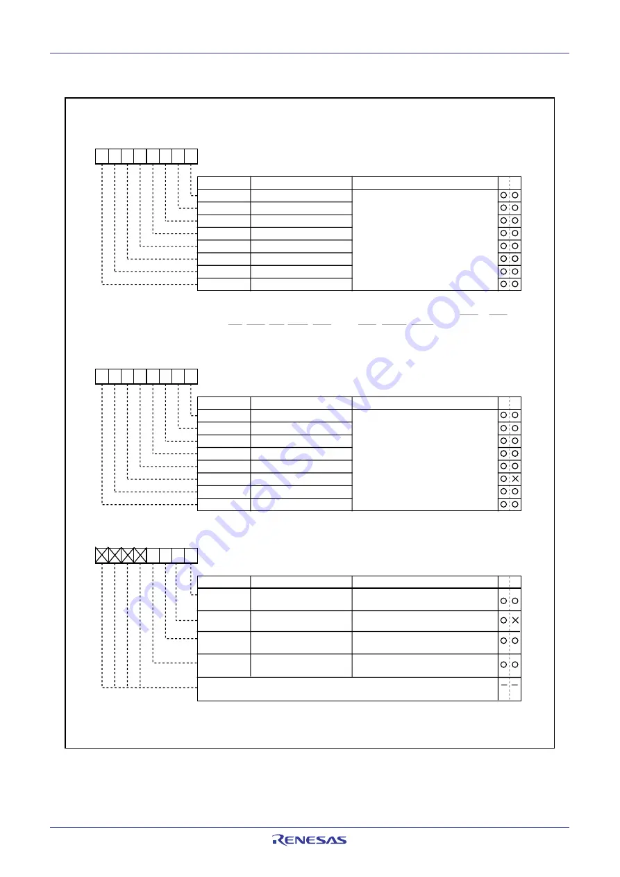
Figure 2.17.4.  Programmable I/O ports-related registers (3)

Port Pi register (Note 2)

Symbol

Address

When reset

Pi (i = 0 to 7, 10)

03E0

16

, 03E1

16

, 03E4

16

, 03E5

16

, 03E8

16

Indeterminate


03E9

16

, 03EC

16

, 03ED

16

, 03F4

16


Indeterminate

Bit name

Function

Bit symbol

W

R

b7

b6

b5

b4

b3

b2

b1

b0

Pi_0

Port Pi

0

 register

Pi_1

Port Pi

1

 register

Pi_2

Port Pi

2

 register

Pi_3

Port Pi

3

 register

Pi_4

Port Pi

4

 register

Pi_5

Port Pi

5

 register

Pi_6

Port Pi

6

 register

Pi_7

Port Pi

7

 register

Data is input and output to and from 
each pin by reading and writing to 
and from each corresponding bit
0 : “L” level data
1 : “H” level data (Note 1)

(i = 0 to 7, 10)

Port P8 register


Symbol

Address

When reset

 P8

03F0

16

Indeterminate

Bit name

Function

Bit symbol

W

R

b7

b6

b5

b4

b3

b2

b1

b0

P8_0

Port P8

0

 register

P8_1

Port P8

1

 register

P8_2

Port P8

2

 register

P8_3

Port P8

3

 register

P8_4

Port P8

4

 register

P8_5

Port P8

5

 register

P8_6

Port P8

6

 register

P8_7

Port P8

7

 register

Data is input and output to and from 
each pin by reading and writing to 
and from each corresponding bit
(except for P8

5

)

0 : “L” level data
1 : “H” level data

A

AA

A

AA

A

AA

A

A

AA

AA

A

AA

A

AA

A

AA

A

AA

A

AA

A

AA

A

AA

A

A

AA

AA

A

AA

A

AA

A

A

AA

AA

A

AA

A

A

AA

AA

A

Note 1: 

Since P7

0

 and P7

1

 are N-channel open drain ports, the data is high-impedance.

Note 2: In memory expansion and microprocessor mode, the contents of 

corresponding port Pi register of pins A

0

 to A

19

, D

0

 to D

15

, CS

0

 to CS

3

RD, WRL/WR, WRH/BHE, ALE, RDY, HOLD, HLDA and BCLK cannot 
be modified.

Port P9 register


Symbol

Address

When reset

 P9

03F1

16

Indeterminate

Bit name

Function

Bit symbol

W

R

b7

b6

b5

b4

b3

b2

b1

b0

P9_0

Port P9

0

 register

VbusDTCT

Vbus detect state bit

P9_2

Port P9

2

 register

P9_3

Port P9

3

 register

0 : “L” level data
1 : “H” level data

A

AA

A

AA

A

AA

A

Nothing is assigned.
Write “0” when writing to these bits. The value is indeterminate if read.

0 : “L” level data
1 : “H” level data

0 : “L” level data
1 : “H” level data

0 : Not powered
1 : Powered (Note 1)

Note 1: This pin cannot be used for GPI/O. This bit reads “0” when Vbus detect is disabled.

Содержание M16C FAMILY

Страница 1: ...ok over all the business of both companies Therefore although the old company name remains in this document it is a valid Renesas Electronics document We appreciate your understanding Renesas Electron...

Страница 2: ...t for an application categorized as Specific or for which the product is not intended where you have failed to obtain the prior written consent of Renesas Electronics The quality grade of each Renesas...

Страница 3: ...hese materials including products and product specifications represents information on the product at the time of publication and is subject to change by Renesas Electronics Corp without notice Please...

Страница 4: ...such as safety systems or equipment or systems for transportation and traffic healthcare combustion control aerospace and aeronautics nuclear power or undersea communication transmission If you are co...

Страница 5: ...supplied until the reset process is completed In a similar way the states of pins in a product that is reset by an on chip power on reset function are not guaranteed from the moment when power is sup...

Страница 6: ...explains a function of the following kind M30245M8 XXXGP M30245MC XXXGP M30245FCGP These products have similar features except for the memories which differ from one product to another Be careful whe...

Страница 7: ...valid When write value can be 0 or 1 Nothing is assigned 3 Terms to use here are explained as follows Nothing is assigned Nothing is assigned to the bit concerned When write set 0 for new function in...

Страница 8: ...8 bit PWM mode selected 31 2 2 12 Precautions for Timer A timer mode 34 2 2 13 Precautions for Timer A event counter mode 35 2 2 14 Precautions for Timer A one shot timer mode 37 2 2 15 Precautions f...

Страница 9: ...with DMAC Transfer 207 2 8 9 Precautions for USB 210 2 9 A D Converter 213 2 9 1 Overview 213 2 9 2 Operation of A D converter one shot mode 218 2 9 3 Operation of A D Converter in one shot mode an e...

Страница 10: ...e 284 2 17 1 Overview of the programmable I O ports usage 284 Chapter 3 Examples of Peripheral Functions Applications 293 3 1 Long Period Timers 295 3 2 Variable Period Variable Duty PWM Output 299 3...

Страница 11: ...able Memories 340 4 4 1 Operation Frequency and Access Time 340 4 4 2 Connecting Low Speed Memory 343 4 4 3 Connectable Memories 346 __________ __________ 4 5 Releasing an External Bus HOLD input and...

Страница 12: ...Chapter 1 Hardware...

Страница 13: ...See M30245 group datasheet...

Страница 14: ...Chapter 2 Peripheral Functions Usage...

Страница 15: ...c cannot be changed in write protect state To change values in the registers put the individual registers in write enabled state 2 Protect register Figure 2 1 1 shows protect register 2 1 Protect Figu...

Страница 16: ...hibited state 4 To change the contents of processor mode register 0 and that of processor mode register 1 follow the same steps as in dealing with system clock control registers and frequency synthe s...

Страница 17: ...an up count or down count in the event counter mode depending on the phase of the two input signals The normal mode or 4 multiplication mode can be selected depending on the phase detective method c...

Страница 18: ...nt at that moment Read it in 16 bit units The data either in one shot timer mode or in pulse width modulation mode is indeterminate 5 Writing to the timer To write to the timer register when a count i...

Страница 19: ...A1 mode register TA1MR Timer A2 mode register TA2MR Timer A3 mode register TA3MR Timer A4 mode register TA4MR Timer A1 interrupt control register TA1IC 004516 004716 005416 005716 005916 038016 03811...

Страница 20: ...set to 000016 the counter does not operate and the Timer Ai interrupt request is not generated When the pulse is se to output the pulse does not output from the TAiOUT pin Note 7 When the Timer Ai re...

Страница 21: ...ulse signal processing function set the select bit to 0 Note Use MOV instruction to write to this register Bit Symbol Bit Name Function R W TA1TGL Timer A1 event trigger select bit Symbol TRGSR Addres...

Страница 22: ...ONSF Address 038216 When reset 0016 One shot start flag b7 b5 b6 b4 b3 b2 b1 b0 0 0 Input on TA0IN is selected Notes 2 3 0 1 Invalid 1 0 TA4 overflow is selected 1 1 TA1 overflow is selected O O TA1OS...

Страница 23: ...ration 1 Setting the count start flag to 1 causes the counter to perform a down count on the count source 2 If an underflow occurs the content of the reload register is reloaded and the count continue...

Страница 24: ...start flag Timer A3 count start flag Timer A4 count start flag b7 b0 Selecting timer mode and functions Timer Ai mode register i 0 to 4 Address 039616 to 039A16 TAiMR i 0 to 4 Selection of timer mode...

Страница 25: ...ns 1 When the count start flag is set to 1 and the TAiIN pin inputs at H level the counter per forms a down count on the count source 2 When the TAiIN pin inputs at L level the counter holds its value...

Страница 26: ...g fC32 by dividing the XCIN by 32 Clock prescaler reset flag Address 038116 CPSRF Clock prescaler reset flag 0 No effect 1 Prescaler is reset When read the value is 0 b7 b0 Setting count start flag Co...

Страница 27: ...0 when interrupt request is accepted or cleared by software 1 Start count 2 Underflow Start count again Item Count source Pulse output function Gate function Set up O O O Internal count source f1 f8...

Страница 28: ...XcIN 32 768kHZ b7 b6 Count source 62 5ns 500ns 2 s 976 56 s 0 0 0 1 1 0 1 1 f1 f8 f32 fC32 Setting divide ratio Can be set to 000016 to FFFF16 b7 b0 b15 b8 b7 b0 Start count Setting clock prescaler r...

Страница 29: ...ective edge of the count source 4 Setting the count start flag to 0 causes the counter to hold its value and to stop 5 If an overflow occurs the content of the reload register is reloaded and the coun...

Страница 30: ...t start flag Address 038216 ONSF Timer A0 event trigger select bit 0 0 Input on TA0IN is selected Note b7 b6 b7 b0 b7 b0 Timer A1 event trigger select bit 0 0 Input on TA1IN is selected Note b1 b0 Tim...

Страница 31: ...s effect from the next effective edge of the count source 4 Even if an overflow occurs the content of the reload register is not reloaded but the count continues At this time the timer Ai interrupt re...

Страница 32: ...nt trigger select bit 0 0 Input on TA0IN is selected Note 2 b7 b6 b7 b0 b7 b0 Timer A1 event trigger select bit 0 0 Input on TA1IN is selected Note 2 b1 b0 Timer A2 event trigger select bit 0 0 Input...

Страница 33: ...e edges of the count source 2 Even if an underflow occurs the content of the reload register is not reloaded but the count continues At this time the timer Ai interrupt request bit goes to 1 3 Even if...

Страница 34: ...8416 UDF Timer A2 two phase pulse signal processing select bit 1 Two phase pulse signal processing enabled Timer A3 two phase pulse signal processing select bit 1 Two phase pulse signal processing ena...

Страница 35: ...he count source 2 Even if an underflow occurs the content of the reload register is not reloaded but the count continues At this time the interrupt request bit goes to 1 3 Even if an overflow occurs t...

Страница 36: ...d Timer A4 two phase pulse signal processing select bit 1 Two phase pulse signal processing enabled Setting divide ratio Can be set to 000016 to FFFF16 b7 b0 b15 b8 b7 b0 Timer A3 register Address 038...

Страница 37: ...reload register again and continues counting The reload timing is in step with the next count source input after the trigger 4 Setting the count start flag to 0 causes the counter to stop and to relo...

Страница 38: ...000116 to FFFF16 Timer A0 register Address 038716 038616 TA0 Timer A1 register Address 038916 038816 TA1 Timer A2 register Address 038B16 038A16 TA2 Timer A3 register Address 038D16 038C16 TA3 Timer A...

Страница 39: ...iOUT pin output level changes from H to L when a set time period elapses At this time the timer Ai interrupt request bit goes to 1 3 The counter reloads the content of the reload register every time P...

Страница 40: ...lect bit One shot start flag Address 038216 ONSF Timer A0 event trigger select bit b7 b6 0 0 Input on TA0IN is selected Note Note 2 Set the corresponding port direction register to 0 Trigger select re...

Страница 41: ...ue is 0 Clock prescaler reset flag Setting clock prescaler reset flag This function is effective when fC32 is selected as the count source Reset the prescaler for generating fc32 by dividing the XCIN...

Страница 42: ...ses are output for one cycle and continues counting 4 Setting the count start flag to 0 causes the counter to hold its value and to stop Also the TAiOUT pin outputs an L level The period of PWM pulses...

Страница 43: ...input signal Note Count source period f XIN 16MHz f XCIN 32 768kHz b7 b6 Count source 62 5ns 500ns 2 s 976 56 s 0 0 0 1 1 0 1 1 f1 f8 f32 fC32 b7 b0 b7 b0 1 Must always be 1 in PWM mode 1 Setting eve...

Страница 44: ...ue is 0 Clock prescaler reset flag Setting clock prescaler reset flag This function is effective when fC32 is selected as the count source Reset the prescaler for generating fc32 by dividing the XCIN...

Страница 45: ...2 Reading the timer Ai register while a count is in progress allows reading with arbitrary timing the value of the counter Reading the timer Ai register with the reload timing shown in Figure 2 2 28...

Страница 46: ...ease note the standards for the differences between the 2 pulses used in the two phase pulse signals input signals to the TAiIN pin and TAiOUT pin i 2 3 4 as shown in Figure 2 2 30 4 When free run typ...

Страница 47: ...will not be changed Enable the Reload function and write to the timer register before counting begins Rewrite the value to the timer register immediately after counting has started If counting up rewr...

Страница 48: ...ocedures Selecting one shot timer mode after reset Changing operation mode from timer mode to one shot timer mode Changing operation mode from event counter mode to one shot timer mode Therefore to us...

Страница 49: ...mode from event counter mode to PWM mode Therefore to use timer Ai interrupt interrupt request bit set timer Ai interrupt request bit to 0 after the above listed changes have been made 3 Setting the...

Страница 50: ...initialize the error flag and the UARTi receive buffer register then receive the data again To initialize the UARTi receive buffer register 1 Set the receive enable bit to 0 disable reception 2 Set t...

Страница 51: ...ad the receive buffer register into a dummy manner Normal mode Writing dummy data to the transmit buffer register makes the reception enabled status ready Continuous receive mode Reading the reception...

Страница 52: ...control register 0 U2C0 UART2 transmit receive control register 1 U2C1 UART2 receive buffer register U2RB UART1 transmit receive mode register U1MR UART1 bit rate generator U1BRG UART1 transmit buffer...

Страница 53: ...or the receive enable bit is set to 0 Bit 15 is set to 0 when all of bits 14 to 12 are set to 0 Bits 14 and 13 are also set to 0 when the lower byte of the UARTi receive buffer register addresses 03AE...

Страница 54: ...Note 3 SMD2 Internal external clock select bit STPS PRY PRYE SLEP Parity enable bit Stop bit length select bit Odd even parity select bit 0 One stop bit 1 Two stop bits 0 Parity disabled 1 Parity enab...

Страница 55: ...ial I O mode and 8 bit UART mode are valid Note 4 The corresponding port register and port direction register are invalid 0 CTS RTS function enabled 1 CTS RTS function disabled 0 LSB first 1 MSB first...

Страница 56: ...request bit goes to 1 Also the first bit of the transmission data is transmitted from the TxDi pin Then the data is transmitted bit by bit from the lower order in synchronization with the falling edg...

Страница 57: ...smission enabled AAAAAAA 2 Confirming CTS AAAAAAA AAAAAAA 3 Start transmission Tc AAAAAAAAAA 4 Transmission is complete AAAAAAAAA 5 Transmit next data Data is set to UARTi transmit buffer register Sto...

Страница 58: ...f8 is selected 1 0 f32 is selected 1 1 Inhibited Transmit register empty flag 0 Data present in transmit register during transmission 1 No data present in transmit register transmission completed Dat...

Страница 59: ...egister 1 UiC1 Address 03AD16 36D16 033D16 32D16 Note Use MOV instruction to write to this register b7 b0 b7 b0 b15 b8 b7 b0 b7 b0 UARTi transmit receive control register 1 UiC1 Address 03AD16 36D16 0...

Страница 60: ...he UARTi transmit buffer register setting the receive enable bit to 1 and the transmit enable bit to 1 makes the data receivable status ready At this time the ________ output from the RTSi pin goes to...

Страница 61: ...re data reception Transmit enable bit 1 Receive enable bit 1 Dummy data write to UARTi transmit buffer register Receive interrupt request bit IR 0 1 Cleared to 0 when interrupt request is accepted or...

Страница 62: ...b1 b0 0 0 f1 is selected 0 1 f8 is selected 1 0 f32 is selected 1 1 Inhibited Transmit register empty flag 0 Data present in transmit register during transmission 1 No data present in transmit regist...

Страница 63: ...ress 033F16 033E16 U2RB UART3 receive buffer register Address 032F16 032E16 U3RB Processing after reading out received data Overrun error flag 0 No overrun error 1 Overrun error found UART0 transmit b...

Страница 64: ...atus becomes ready which informs the transmis ________ sion side that the reception has become ready The output level of the RTSi pin goes to H ________ ________ when reception starts So if the RTSi p...

Страница 65: ...ading the contents of the UARTi receive buffer register and receives the 7th bit of the next data item and then the overrun error flag is set to 1 In this instance the next data is written to the UART...

Страница 66: ...2SP 1ST 8DATA 1PAR 1SP 1ST 8DATA 1PAR 2SP Transfer data length 9 bits 1ST 9DATA 1SP 1ST 9DATA 2SP 1ST 9DATA 1PAR 1SP 1ST 9DATA 1PAR 2SP ST Start bit DATA Character bit Transfer data PAR Parity bit SP...

Страница 67: ...e flag This error occurs when the serial interface starts receiving the next data item before reading the contents of the UARTi receive buffer register and receives the bit preceding the final stop bi...

Страница 68: ...CTS pin input level is detected when transmission reception starts so if the level is gone to H while transmission reception is in progress transmission recep tion stops at the next data _______ _____...

Страница 69: ...ted by connecting SIM card The following examples are described in section 2 4 4 and 2 4 5 Transmission WITH direct format Reception WITH direct format 6 Input to the serial I O and the direction regi...

Страница 70: ...r U3TB UART3 transmit receive control register 0 U3C0 UART3 transmit receive control register 1 U3C1 UART3 receive buffer register U3RB UART2 transmit receive mode register U2MR UART2 bit rate generat...

Страница 71: ...enable bit is set to 0 Bit 15 is set to 0 when all of bits 14 to 12 are set to 0 Bits 14 and 13 are also set to 0 when the lower byte of the UARTi receive buffer register addresses 03AE16 036E16 033E1...

Страница 72: ...ternal external clock select bit STPS PRY PRYE SLEP Parity enable bit Stop bit length select bit Odd even parity select bit 0 One stop bit 1 Two stop bits 0 Parity disabled 1 Parity enabled 1 0 0 Tran...

Страница 73: ...d 8 bit UART mode are valid Note 4 The corresponding port register and port direction register are invalid 0 CTS RTS function enabled 1 CTS RTS function disabled 0 LSB first 1 MSB first UARTi transmit...

Страница 74: ...g to this bit The value is indeterminate when read Bus collision interrupt request cause select bit 0 Bus collision interrupt request cause select bit 1 0 One edge 1 Two edges 0 One edge 1 Two edges I...

Страница 75: ...e bit to 1 and writing transmission data to the UARTi transmit buffer register readies the data transmissible status ________ ________ 2 When input to the CTSi pin goes to L transmission starts the CT...

Страница 76: ...ped pulsing because transfer enable bit 0 Stop bit Data is set in UARTi transmit buffer register Transferred from UARTi transmit buffer register to UARTi transmit register Tc Transfer clock When confi...

Страница 77: ...CMOS output 1 TxDi SDAi and SCLi pin is N channel open drain output CTS RTS disable bit 0 CTS RTS function enabled UARTi transmit receive control register 0 UiC0 Address 03AC16 36C16 033C16 32C16 Tran...

Страница 78: ...t buffer register Address 032B16 032A16 U3TB Setting transmission data Note Use MOV instruction to write to this register Writing transmit data Note Setting transmission data Setting transmission data...

Страница 79: ...Selected 1 Setting the receive enable bit to 1 readies data receivable status At this time output from ________ the RTSi pin goes to L level to inform the transmission side that the receivable status...

Страница 80: ...ceive complete flag RTSi Stop bit 1 0 0 1 H L Timing of transfer data 8 bits long applies to the following settings Transfer data length is 8 bits Parity is disabled One stop bit RTS function is selec...

Страница 81: ...pin is CMOS output 1 TxDi SDAi and SCLi pin is N channel open drain output CTS RTS disable bit 0 CTS RTS function enabled UARTi transmit receive control register 0 UiC0 Address 03AC16 36C16 033C16 32C...

Страница 82: ...RTi transmit receive control register 1 UiC1 Address 03AD16 36D16 033D16 32D16 b7 b0 Receive enable bit 1 Reception enabled Note 1 UARTi transmit receive control register 1 UiC1 Address 03AD16 36D16 0...

Страница 83: ...e UiMR register Change the setting of bits SMD2 to SMD0 from 0002 serial I O disabled to 1012 UART mode transfer data length 8 bits Change the setting of bits SMD2 to SMD0 from 0012 clock synchronous...

Страница 84: ...SB parity bit and stop bit s 3 When the stop bit s is are transmitted the transmit register empty flag goes to 1 which indicates that transmission is completed At this time the UARTi i 0 to 3 transmit...

Страница 85: ...e D0 D1 D2 D3 D4 D5 D6 D7 ST P SP Shown in are bit symbols Tc Transfer clock SP Stop bit Since a parity error occurred the L level returns from SIM card Detects the level using an interrupt routine De...

Страница 86: ...smit receive control register 0 i 0 to 3 UARTi transmit receive control register 0 UiC0 Address 03AC16 36C16 033C16 32C16 Data logic select bit Must be 0 no reverse in direct format UARTi transmit int...

Страница 87: ...32916 UiBRG i 0 to 3 Transmission enabled Transmit enable bit 1 Transmission enabled 1 Writing transmit data Note Setting transmission data UART0 transmit buffer register Address 03AB16 03AA16 U0TB UA...

Страница 88: ...MSB and stop bit s 3 When the stop bit s is are received the content of the UARTi i 0 to 3 receive register is transmitted to the UARTi i 0 to 3 receive buffer register At this time the receive compl...

Страница 89: ...from TxDi RXDi Note Read to receive buffer Read to receive buffer D0 D1 D2 D3 D4 D5 D6 D7 ST P Signal line level Note D0 D1 D2 D3 D4 D5 D6 D7 ST P SP Note TxDi and RxDi are connected in the manner of...

Страница 90: ...1 Transfer data 8 bits long Stop bit length select bit 0 One stop bit Parity enable bit 1 Parity enabled TXD RXD I O polarity reverse bit Usually set to 0 Odd even parity select bit Valid when bit 6...

Страница 91: ...Received data Overrun error flag 0 No overrun error 1 Overrun error found Framing error flag 0 No framing error 1 Framing error found Parity error flag 0 No parity error 1 Parity error found Error su...

Страница 92: ...on In the case of setting a value equal to or less than 1 256 X 1 16 in the division rate of UARTi clock UARTi clock signal within microprocessor UART clock within SIM card f1 x x f1 x x flip flop x L...

Страница 93: ...19 Example of connection Clock generator UART TAjOUT flip flop M30245 f1 CLK UART clock UART 1 F D SIM card internal clock frequency division ratio SIM CARD External clock Timer Ak counter flip flop T...

Страница 94: ...5952 1487 1 16 17856 2231 1 32 11904 2975 1 32 35712 4463 1 64 23808 5951 1 64 71424 8927 558 1 558 1488 1 1488 2 279 2 744 185 4 4 372 92 8 8 186 16 16 93 1 2 1116 278 1 2 2976 371 1 4 2232 557 1 4...

Страница 95: ...7 1 16 17856 4463 1 32 11904 2975 1 32 35712 8927 1 64 23808 5951 1 64 71424 17855 558 1 558 1488 1 1488 371 2 279 2 744 185 4 4 372 92 8 8 186 16 16 93 1 2 1116 278 1 2 2976 743 1 4 2232 557 1 4 5952...

Страница 96: ...rrupt request bit becomes 1 and a fault error interrupt is generated 4 How to deal with an error When the fault error flag is set to 0 output is restored to the clock output and data output pins In th...

Страница 97: ...utting reception data at rising edge of transfer clock clock delay slave mode 6 Input to the serial interface special function and the direction register To input an external signal to the serial inte...

Страница 98: ...U3RB UART2 transmit receive mode register U2MR UART2 bit rate generator U2BRG UART2 transmit buffer register U2TB UART2 transmit receive control register 0 U2C0 UART2 transmit receive control registe...

Страница 99: ...e set to 0002 or the receive enable bit is set to 0 Bit 15 is set to 0 when all of bits 14 to 12 are set to 0 Bits 14 and 13 are also set to 0 when the lower byte of the UARTi receive buffer register...

Страница 100: ...de select bit Note 3 SMD2 Internal external clock select bit STPS PRY PRYE SLEP Parity enable bit Stop bit length select bit Odd even parity select bit 0 One stop bit 1 Two stop bits 0 Parity disabled...

Страница 101: ...ynchronous serial I O mode and 8 bit UART mode are valid Note 4 The corresponding port register and port direction register are invalid 0 CTS RTS function enabled 1 CTS RTS function disabled 0 LSB fir...

Страница 102: ...nable bit Bus busy flag Arbitration lost detecting flag control bit IICM ABC BBS LSYN ABSCS ACSE SSS Nothing is assigned Write 0 when writing to this bit The values are indeterminate when read R W ALS...

Страница 103: ...he amount of delay varies with the load on SCLi and SDAi pins When external clock is selected delay is increased by approximately 100ns 0 0 0 No delay 0 0 1 1 to 2 cycle of UiBRG count source 0 1 0 2...

Страница 104: ...L L hold enabled Note 2 Note 1 These bits automatically become 0 when a start condition is generated Note 2 This bit is unavailable when SCLi is external clock IFSR0 IFSR1 IFSR2 IFSR6 IFSR7 R W b7 b6...

Страница 105: ...missible status ready 3 In synchronization with the first falling edge of the transfer clock transmission data held in the UARTi transmit buffer register is transmitted to the UARTi transmit register...

Страница 106: ...Output L at the receiver side IC AAAAAAAA AAAAAAAA 2 Transmission enabled AAAAAAA AAAAAAA 3 Start transmission Tc AAAAAAAAAA AAAAAAAAAA 4 Transmission is complete AAAAAAAAA AAAAAAAAA 5 Transmit next d...

Страница 107: ...0 TxDi SDAi and SCLi pin is CMOS output 1 TxDi SDAi and SCLi pin is N channel open drain output CLK polarity select bit 0 Transmission data is output at falling edge of transfer clock and reception d...

Страница 108: ...16 033D16 32D16 UARTi bit rate generator Address 03A916 036916 033916 032916 UiBRG i 0 to 3 Note Use MOV instruction to write to this register Write to UARTi bit rate generator when transmission recep...

Страница 109: ...re 2 5 11 shows the operation timing and Figures 2 5 12 and 2 5 13 show the set up procedures ____ 1 Set an SS port of the transmitter side IC to output L level 2 Writing dummy data to the UARTi trans...

Страница 110: ...sferred from UARTi receive register to UARTi receive buffer register 2 Reception enabled 3 Start reception 4 Reception is complete Read out from UARTi receive buffer register Transferred from UARTi tr...

Страница 111: ...pleted Data output select bit Note 2 0 TxDi SDAi and SCLi pin is CMOS output 1 TxDi SDAi and SCLi pin is N channel open drain output CLK polarity select bit 0 Transmission data is output at falling ed...

Страница 112: ...ag 0 No overrun error 1 Overrun error found UART0 receive buffer register Address 03AF16 03AE16 U0RB UART1 receive buffer register Address 036F16 036E16 U1RB UART2 receive buffer register Address 033F...

Страница 113: ...mit buffer register makes data transmissible status ready 3 In synchronization with the first falling edge of the transfer clock transmission data held in the UARTi transmit buffer register is transmi...

Страница 114: ...o UARTi transmit buffer register Shown in are bit symbols Transmit interrupt request bit IR Transmit buffer empty flag 0 1 0 1 Transfer clock 0 1 0 1 2 Transmission enabled 3 Start transmission 4 Tran...

Страница 115: ...completed Data output select bit Note 2 0 TxDi SDAi and SCLi pin is CMOS output 1 TxDi SDAi and SCLi pin is N channel open drain output CLK polarity select bit 0 Transmission data is output at falling...

Страница 116: ...ansmit receive control register 1 UiC1 Address 03AD16 36D16 033D16 32D16 UARTi transmit receive control register 1 UiC1 Address 03AD16 36D16 033D16 32D16 UART0 transmit buffer register Address 03AB16...

Страница 117: ...items are described below Figure 2 5 17 shows the operation timing and Figures 2 5 18 and 2 5 19 show the set up procedures ____ 1 An SSi port is input L level which outputs from the transmitter side...

Страница 118: ...buffer register Receive interrupt request bit IR 0 1 Cleared to 0 when interrupt request is accepted or cleared by software Shown in are bit symbols Reception data is taken in Transferred from UARTi r...

Страница 119: ...output select bit Note 2 0 TxDi pin is CMOS output 1 TxDi pin is N channel open drain output CLK polarity select bit 0 Transmission data is output at falling edge of transfer clock and reception data...

Страница 120: ...ror 1 Overrun error found UART0 receive buffer register Address 03AF16 03AE16 U0RB UART1 receive buffer register Address 036F16 036E16 U1RB UART2 receive buffer register Address 033F16 033E16 U2RB UAR...

Страница 121: ...ons The transmitter receiver must change channels on every WS transition The number of SCKs within a WS high low period is set as the channel width The channel width can be selected from among 16 bits...

Страница 122: ...ted by the WS polarity select bit in the Serial Sound Interface x mode register 1 7 WS delay select function Either of the following modes may be selected for the channel change timing Normal WS mode...

Страница 123: ...0TXB Serial Sound Interface 0 receive buffer register SS0RXB Serial Sound Interface 0 RF register SS0RF Reserved Serial Sound Interface 1 mode register 0 SSI1MR0 Serial Sound Interface 1 mode register...

Страница 124: ...6 O O R W b7 b8 b15 b0 b7 b0 SSIxRXB x 0 1 O O 000016 000016 Serial Sound Interface x transmit buffer register Serial Sound Interface x receive buffer register Function Symbol Address When reset Funct...

Страница 125: ...P WSP WSDLY Rate feedback counter source SCK polarity select bit WS polarity select bit WS delay select bit 0 SCK 1 WS 0 Falling edge 1 Rising edge 0 Delayed WS 1 Normal WS R W b7 b0 b6 b5 b4 b3 b2 b1...

Страница 126: ...ffer OPERATION First Word Write Third Word Write Second Word Write Fourth Word Write Byte 1 Byte 0 First byte Second byte Fifth byte Sixth byte Right Buffer Byte 1 Byte 0 Third byte Fourth byte Sevent...

Страница 127: ...0x00 DMA1 STOP Setting example Audio transmission can be set before or after audio reception The DMA to use is set DMA0 audio data transmission and DMA1 audio data reception dm0ic 0x06 DMA completion...

Страница 128: ...6bit Tx enable Rx enable MSB justified endif Serial Sound Interface activation routine for 24 bits ifdef OUT_Q_BIT_NO_24 ssi1mr0 0x01 SSIEN 1 ssi1mr0 0xd1 24bit MSB justified ssi1mr1 0x21 SCK neg WS n...

Страница 129: ...8MHz Max192 Fs 9 2MHz XMTEN SCKP 1 WSP 0 SCKP 0 WSP 0 SCKP 1 WSP 1 SCKP 0 WSP 1 WSDLY 1 XMTFMT 0 MSB first XMTFMT 1 LSB first Fs 48 kHz or 44 1kHz Serial Sound Interface timing 1 Serial Sound Interfac...

Страница 130: ...SCKP 1 WSP 0 SCKP 0 WSP 0 SCKP 1 WSP 1 SCKP 0 WSP 1 SCK Min 64 Fs 2 8MHz Max192 Fs 9 2MHz RFMT1 0 MSB first RFMT1 1 LSB first Fs 48 kHz or 44 1kHz Serial Sound Interface timing 3 WS RXEN SCKP 1 WSP 0...

Страница 131: ...6 3 Precautions for Serial Sound Interface For flash memory version SSI transmission data must be latched as the following timing by a receiver SCKP 0 falling edge within 3 BCLK cycles from the rising...

Страница 132: ...diagram FSP FSM FSC f XIN fPIN fVCO fSYN fUSB FSD FSCCR FSCCR0 USBC5 EN Data Bus Frequency Multiplier 03DF16 03DC16 03DD16 03DE16 03DB16 8 Bit 8 Bit 8 Bit Frequency Divider Prescaler LS 1 Related Reg...

Страница 133: ...Note 1 Recommended Note 2 Bits 6 and 5 are set to bit 6 bit 5 1 1 at reset When using the frequency synthesizer we recommend to set to bit 6 bit 5 1 0 O O O O O O O O O O O O O O 0 0 b6 b5 0 0 Disabl...

Страница 134: ...es fPIN fPIN f XIN 2 n 1 n FSP value Bit Symbol Bit Name Function R W Symbol FSM Address 03DD16 When reset 111111112 b7 b5 b6 b4 b3 b2 b1 b0 FSM O O Frequency synthesizer multiplier value Generates fV...

Страница 135: ...t is 0 unlocked 6 Enable USB clock 7 After waiting four cycles of the or greater the USB enable bit should be set to 1 A minimum delay of 250ns is needed before performing any other USB related regist...

Страница 136: ...frequency synthesizer divide register FSD When the frequency synthesizer divider register is set to 255 division is disabled and fSYN fVCO Table 2 7 3 shows some examples of how the frequency synthes...

Страница 137: ...e of the registers should be changed 5 When using the frequency synthesizer connect a low pass filter to the LPF terminal 6 The following setup for the frequency synthesizer should be done after hardw...

Страница 138: ...cern 2 types including the one for the host side PC Hub to control the connected peripheral devices and the other for the peripheral device side Device which is con nected to the real machine Further...

Страница 139: ...es real time 2 Communication Protocol Host CPU has the initiative for the entire USB communication Even when data are transmitted to the host from the device the host gives the right of use to the dev...

Страница 140: ...he time of data transfer Hand Shake Packet Packet to use at the transaction which controls flow Figure 2 8 2 Kinds of packet PID name SETUP IN OUT SOF DATA0 DATA1 ACK NAK STALL Table 2 8 1 List of USB...

Страница 141: ...ts of transactions IN DATA0 1 AA AA NAK AAA AAA STALL AAA AAA ACK OUT AA AA ACK AA AA NAK AA AA STALL DATA0 1 SETUP AA AA ACK DATA0 IN DATA0 OUT DATA0 AAAA AAAA AAAA AAAA IN transaction idle state OUT...

Страница 142: ...complete one processing In control transfer use of endpoint 0 has been specified The communication sequence of control transfer is shown in Figure 2 8 4 AAAAA AAAAA SETUP DATA0 IN AAAA AAAA DATA1 0 A...

Страница 143: ...ntrol Data Transfer In setup stage host notifies the device that it is no control data transfer Then in status stage IN transaction is executed that the device transmits an empty packet of data length...

Страница 144: ...The M30245 group has normally received a data packet and then returns ACK handshake Normal receiving is the status which is free of any bit stuffing error or CRC error and which data PID have been cor...

Страница 145: ...host CPU to the device isochro nous OUT transactions are repeated Isochronous transaction does not have the handshake phase The data packet consists only of DATA0 Toggling with DATA1 is not performed...

Страница 146: ...al has been received from the host CPU It is responded as default address 0 This is the unconfigured state configuration 0 Address State This is the state which the SET_ADDRESS standard device request...

Страница 147: ...SB suspend interrupt Resume detected USB resume interrupt Suspend detected USB suspend interrupt Resume detected USB resume interrupt Suspend detected USB suspend interrupt Resume detected USB resume...

Страница 148: ...USB ISO control register USBISOC USB endpoint enable register USBEPEN USB DMA0 request register USBDMA0 USB EP0 control status register EP0CS USB EP0 max packet size register EP0MP USB EP0 OUT write c...

Страница 149: ...r USB endpoint x x 0 4 OUT FIFO data register USB function interrupt status register USB function interrupt clear register USB function interrupt enable register USB frame number register USB power ma...

Страница 150: ...ling the USB clock ________ USB SOF port select bit This bit is used to enable disable a SOF signal output on the P92 pin Set this bit to 1 when using the USB SOF signal In this case set the port P92...

Страница 151: ...ble becomes a attach state artificially since the Uvcc pin voltage is supplied to the P90 and D line is pulled up After frequency synthesizer is stabilized set 1 attach state to this bit Vbus detect e...

Страница 152: ...Figure 2 8 11 USB endpoint enable register Bit Symbol Bit Name Function R W Must always be 0 Symbol USBEPEN Address 028E16 When reset 000016 USB Endpoint Enable register b7 b15 b8 b0 EP1_OUT b7 b0 EP1...

Страница 153: ...02E216 02E616 02EA16 02EE16 02F216 When reset N A USB Endpoint x OUT FIFO Data register b7 b15 b8 b0 DATA_15 0 b7 b0 EP0 OUT FIFO Data O X Note 1 Writing to this register might cause a system error N...

Страница 154: ...ock status bit If the frequency synthesizer is in unlock state waiting for 0 1ms and rechecking are repeated Setting of the USB function control unit 7 Set the USBC5 to 1 to enable the USB clock 8 Set...

Страница 155: ...FSP Frequency synthesizer prescaler FSM Frequency synthesizer multiplier FSD Frequency synthesizer divider RESET FSE LS USBC5 USBC7 Enable USB function control unit Enable frequency synthesizer Wait f...

Страница 156: ...iting to processor mode registers 0 and 1 0 Write inhibited Reserved bit Checking the frequency synthesizer locked status bit It is necessary to recheck after a wait of 0 1ms if it is 0 Wait for 3ms F...

Страница 157: ...6 USBAD Port 90 Second 0 Normal mode for Port 90 1 Forces Port 90 to operate as pull up for D Attach Detach 0 Detach 1 Attach Reserved bit USB clock enabled USB control register Address 000C16 USBC US...

Страница 158: ...gest buffer size Double buffer mode 0 Double buffer mode disabled 1 Double buffer mode enabled Continuous transfer mode Note 0 Continuous transfer disabled 1 Continuous transfer enabled Note Valid whe...

Страница 159: ...IFO enable bit 0 Disabled 1 Enabled Endpoint 2 IN FIFO enable bit 0 Disabled 1 Enabled Endpoint 3 OUT FIFO enable bit 0 Disabled 1 Enabled Endpoint 3 IN FIFO enable bit 0 Disabled 1 Enabled Endpoint 4...

Страница 160: ...pin is used for the Vbus detect function When operating the USB in self powered mode connect the Vbus line from the USB connector to the VbusDTCT pin For enable disable of the Vbus detect function se...

Страница 161: ...set to 1 at the corresponding endpoint that has been enabled by USB function interrupt enable register in the following cases The endpoint is enabled from a disabled state One buffer data is successf...

Страница 162: ...when the request of interrupt which set the enable bit to 1 occurs The configuration of USB function interrupt enable register is shown in Figure 2 8 23 Figure 2 8 21 USB function interrupt status re...

Страница 163: ...flag Clear EP2 OUT interrupt status flag Clear EP3 IN interrupt status flag Clear EP3 OUT interrupt status flag Clear EP4 IN interrupt status flag Clear EP4 OUT interrupt status flag Reserved Clear e...

Страница 164: ...This is the read only register The configuration of USB frame number register is shown in Figure 2 8 24 Figure 2 8 24 USB frame number register Bit Symbol Bit Name Function R W 0 when read Symbol USBF...

Страница 165: ...nt 0 interrupt occurs when one of the following events occur A data is successfully received A data is successfully transmitted The DATA_END bit of the EP0CS register is cleared to 0 The SETUP_END fla...

Страница 166: ...t enable register USBEPEN address 028E16 is set to 1 The endpoint is enabled from a disabled state A data is successfully transmitted AUTO FLUSH of hardware has been executed or FLUSH bit of correspon...

Страница 167: ...ower management register USBPM address 028216 is set when the USB function control unit has detected suspend signal on the USB bus line or not detected any bus activity on the D D line for at least 3m...

Страница 168: ...ime that the SOF signal is received from the host the P92 outputs Low for about 166ns two cycles of the 12MHz USB clock When using the USB SOF interrupt set the interrupt priority level at USB SOF int...

Страница 169: ...a transmit receive or on occurrence of an error such as overrun underrun When using the USB function interrupt set the interrupt priority level at USB function interrupt control register address 005D1...

Страница 170: ...6 EP1 IN interrupt status flag EP1 OUT interrupt status flag EP2 IN interrupt status flag EP2 OUT interrupt status flag EP3 IN interrupt status flag EP3 OUT interrupt status flag EP4 IN interrupt stat...

Страница 171: ...rd to USBIC RAM bit8 1 USB error interrupt routine RAM bit1 1 or RAM bit3 1 or RAM bit5 1 or RAM bit7 1 USB endpoint x OUT interrupt routine RAM bit0 1 or RAM bit2 1 or RAM bit4 1 or RAM bit6 1 USB en...

Страница 172: ...USB suspend status flag is set Simultaneously the USB suspend interrupt request occurs This flag is automatically cleared in the following cases The active signal from the host CPU has been detected o...

Страница 173: ...uspend state flag 0 Not in suspend state 1 In suspend state Note 1 O Reserved WAKEUP Remote wakeup 0 End remote wakeup signal 1 Remote wakeup signaling Note 3 O O Note 1 This flag is cleared when WAKE...

Страница 174: ...r related registers when the USB clock has been disabled in the suspend state 2 During the bus power supply operation as a low power device control it to reduce the total driving current to 500 A or b...

Страница 175: ...me interrupt follow the procedure below 1 Return the USB function control unit Refer to the next page 2 Enable other functions as circumstances demand Returning by Remote Wakeup When clock operation i...

Страница 176: ...ol register address 03DC16 1 Set frequency synthesizer enable bit of frequency synthesizer control register to 1 2 Wait for 3ms 3 Check that frequency synthesizer lock status bit of frequency synthesi...

Страница 177: ...SB control register Address 000C16 USBC USB clock enable bit 0 Disable 48MHZ clock supply disabled Detection of USB suspend interrupt request Continued to the next page Setting the interruppt for retu...

Страница 178: ...quest processing routine 2 Stop all clocks System clock control register 1 Address 000716 CM1 All clock stop control bit 1 All clocks off stop mode Insert at least four NOPs following JMP B instructio...

Страница 179: ...1 Enabled Detection of USB resume interrupt request Clearing the protect Protect register Address 000A16 PRCR Enable bit for writing to system clock control registers 0 and 1 and frequency synthesizer...

Страница 180: ...USB address register maintains 7 bits addresses of the USB function control unit that are allocated by the host CPU The USB function control unit of the M30245 group responds to the token packet for t...

Страница 181: ...flag is cleared by setting 1 to CLR_SETUP bit DATA_END Flag This flag shows the status phase control of control transfer After the status phase is started or when a new SETUP packet is received this...

Страница 182: ...it data to the host CPU exists IN_BUF_RDY bit is cleared to 0 and the IN FIFO data is destroyed Discontinue access to FIFO and process the preceding setup Also when a new SETUP packet is received righ...

Страница 183: ...ing of the FORCE_STALL flag When this bit is written to 1 the FORCE_STALL flag is cleared to 0 SEND_STALL bit This bit controls the STALL response to the host CPU To responds with STALL when an invali...

Страница 184: ...ta set ready for transmit 1 Data set ready for transmit 0 No setup packet ready for unload 1 Data set ready for transmit 0 DATA_END not set by CPU or DATA END is set by CPU then status phase starts 1...

Страница 185: ...receive completes read this register and determine the number of bytes to be read from OUT FIFO This register value is not decremented even if the data is read from OUT FIFO When CLR_OUT_BUF_RDY bit...

Страница 186: ...ntrol transfer by software When the SETUP packet is received the USB endpoint 0 interrupt occurs regardless of setting of continuous transfer mode enable bit The OUT_BUF_RDY flag and the SETUP flag ar...

Страница 187: ...set to 1 After writing the last data packet in IN FIFO set SET_IN_BUF_RDY bit to 1 and simultaneously set SET_DATA_END bit to 1 Both the IN_BUF_RDY flag and DATA_END flag are set to 1 When the DATA_E...

Страница 188: ...pleted USB address register is rewritten into the address written in above mentioned 1 When the status phase is not normally completed USB address register is not rewritten When the device is in the a...

Страница 189: ...ading of receive data USB endpoint 0 OUT FIFO data register EP0O Address 02E216 The data equal to receive byte count are read setup packet is 8 byte Store the receive data in user definition RAM To pr...

Страница 190: ...address register Note 1 Note 1 Only the lower 1 byte of the receive device address should be set Setting of USB endpoint 0 control and status register USB endpoint 0 control and status register EP0CS...

Страница 191: ...eption is compete SETUP flag 0 Data packet reception 1 SETUP packet reception Reading of receive data USB endpoint 0 OUT FIFO data register EP0O Address 02E216 The data equal to receive byte count are...

Страница 192: ...IN_BUF_RDY flag to 1 SET_DATA_END bit 1 Set DATA_END flag to 1 Completion of GET_CONFIGURATION request Continued from previous page Note 1 Set the SET_IN_BUF_RDY bit and the SET_DATA_END bit simultane...

Страница 193: ...iving the packet data The data receive from the host CPU is controlled based on the communication status of endpoints 1 to 4 OUT The default of endpoints 1 to 4 is bulk transfer Each endpoint should b...

Страница 194: ...s transfer When OUT FIFO is not empty and disables receiving at start of the OUT token from the host CPU occurrence of an overrun is recognized setting this bit to 1 Clear this flag by writing 1 to CL...

Страница 195: ...nside the OUT FIFO The receive data may be destroyed if this bit is set to 1 during USB transfer Read the OUT_BUF_STS1 and OUT_BUF_STS0 flags and confirm that there are data in the OUT FIFO and then s...

Страница 196: ...fer 0 1 Single buffer mode N A Double buffer mode N A 1 0 Single buffer mode N A Double buffer mode one data set in the OUT buffer 1 1 Single buffer mode one data set in the OUT buffer Double buffer m...

Страница 197: ...d from OUT FIFO This register value is not decremented even if the data are read from USB endpoint x OUT FIFO register When this register is read while there are two buffer data in OUT FIFO in the dou...

Страница 198: ...cket is received When continuous receive mode is enabled the BUF_SIZ has to be equal to an integral multiple of the EPxOMP Further the user s system has to be comprehended beforehand that the receive...

Страница 199: ...he USB function control unit writes the receive data from the host PC in OUT FIFO sequentially by one packet size the maximum packet size set in the EPxOMP re ceives continuously until one buffer full...

Страница 200: ...ceive packet data fetch Note 2 At this time the OUT FIFO status OUT_BUF_STS1 and OUT_BUF_STS0 flags are updated enabling a receive of the next one packet data Note 2 In Single Buffer Mode The OUT_BUF_...

Страница 201: ...B2 0 specification are automatically performed When the OUT token is received from the host CPU while there are already data in OUT FIFO and packet data cannot be received an overrun error occurs At t...

Страница 202: ...UF_STS0 flags states when reading data from the OUT FIFO Based on these flags states judge whether there are receive data in the OUT FIFO Be sure to read the byte count of data specified by USB endpoi...

Страница 203: ...hen the data count equal to one packet is read from the OUT FIFO Process of USB endpoint x OUT packet fetch 1 Confirming of whether one packet is received in the OUT FIFO check the OUT_BUF_STS0 and th...

Страница 204: ...should be initialized in order to use other transfer modes The transmit of endpoints 1 to 4 can select the following functions Continuous Transmit Mode This function is used for transmitting data at...

Страница 205: ...chronous transfer The bit is valid only for the IN endpoints 1 to 4 in isochronous transfer While ISO_UPDATE bit 0 and ISO bit 1 the USB function control unit at the time of receiving of an IN token f...

Страница 206: ...OF enable bit is 1 With this flag being set to 1 an artificial SOF receive has occurred by the artificial SOF function This flag is cleared by setting 1 to CLR_ART_SOF bit Artificial SOF status clear...

Страница 207: ...continuous transfer enable has been written in the FIFO However when a short packet has been written at the time of AUTO_SET enable these flags are not automatically updated In such cases set SET_IN_...

Страница 208: ...ags are updated to 012 This indicates that one more buffer data is left inside the IN FIFO The transmit data may be destroyed if this bit is set to 1 during USB transfer On completing one buffer data...

Страница 209: ...t Symbol Bit Name Function R W Symbol EPxICS x 1 4 Address When reset USB Endpoint x IN Control and Status register b7 b15 b8 b0 INxCSR0 INxCSR1 INxCSR2 INxCSR3 INxCSR4 INxCSR5 INxCSR6 INxCSR7 INxCSR8...

Страница 210: ...t CPU change the endpoint x IN maximum packet size value by writing in this register Set a packet size value specified for every transfer type to be used The configuration of USB endpoint x x 1 to 4 I...

Страница 211: ...ize set in the EPxIMP it is transmitted as a short packet When continuous transmit mode is enabled the value set in the BUF_SIZ has to be equal to an integral multiple of the maximum packet size Pay a...

Страница 212: ...Contents of the internal write pointer cannot be read For transmitting an empty packet with 0 data length do not write data to the IN FIFO 3 Set SET_IN_BUF_RDY bit to 1 At this time the IN FIFO status...

Страница 213: ...ing that one more transmit data is left inside the IN FIFO When there is one packet data Note 2 in IN FIFO the IN_BUF_STS0 and IN_BUF_STS0 flags are updated from 012 to 002 when the data are transmitt...

Страница 214: ...an error interrupt request occurs INTST8 is set to 1 When IN token is received from the host CPU while there are packet data in IN FIFO data are transmitted At this time the IN FIFO status is updated...

Страница 215: ...s 1 to 4 Transmit Continu ous transfer is valid for the bulk transfer only Rate Feedback Interrupt Transfer In real application transmit data to the host CPU has to be always prepared Prepare one tran...

Страница 216: ...e re transmitted in the next IN token the same data are transmitted in the same toggle 5 Precautions for Transmit Writing to IN FIFO Be sure to confirm that there is a space in the IN FIFO before writ...

Страница 217: ...ffer data in continuous transfer mode Note 3 When the AUTO_SET bit is set to 1 this bit is automatically set to 1 when the data count set by maximum packet size register is written to the IN FIFO When...

Страница 218: ...y to 1 bit When multiple bits are simultaneously set to 1 the setting becomes invalid Other DMA related registers also need to be set before a valid value is set for example 000112 USB0 USB1 USB2 USB3...

Страница 219: ...more packets are received in OUT FIFO There is no selection of USB DMAx x 0 to 3 request register 0016 Event Any one of endpoint x x 1 to 4 OUT FIFO read request select bit in USB DMAx x 0 to 3 reque...

Страница 220: ...e the space of one or more packets in the IN FIFO There is no selection of USB DMAx x 0 to 3 request register 0016 Event Any one endpoint x x 1 to 4 IN FIFO write request select bit in USB DMAx x 0 to...

Страница 221: ...of the peripheral components need to be adjusted according to differences in characteristic impedance and layout of the mount printed circuit board Therefore fully evaluate on the system in use and ob...

Страница 222: ...lue of resistance and capacitor and the configuration will depened on the layout of printed circuit board USB Transceiver Frequency synthesizer P90 control Connect to ATTACH or UVCC 0 47 F 1 5k Figure...

Страница 223: ...ter software reset contents of all the USB related registers are retained While the USB clock is held disabled in suspend mode writing in the USB internal registers other than USBC USBAD and frequency...

Страница 224: ...two or more specified pins This mode is different from the repeated sweep mode 0 in that weights can be assigned to specifing pins control the number of conversion times 2 Operation clock The operatio...

Страница 225: ...on Vref X n 28 Vref X 0 5 210 n 1 to 255 0 n 0 c A D conversion by external trigger The user can select software or an external pin input to start A D conversion d Connecting or cutting Vref Cutting V...

Страница 226: ...516 03C616 03C716 03C816 03C916 03CA16 03CB16 03CC16 03CD16 03CE16 03CF16 03D416 03D516 03D616 03D716 03D816 AD register 7 AD7 AD register 0 AD0 AD register 1 AD1 AD register 2 AD2 AD register 3 AD3 A...

Страница 227: ...ADTRG trigger 0 A D conversion disabled 1 A D conversion enabled Note 4 0 fAD 3 or fAD 4 is selected 1 fAD or fAD 2 is selected O O O O O O O O O O O O O O O O b2 b1 b0 b4 b3 Bit Symbol Function R W...

Страница 228: ...6 Indeterminate ADi i 3 to 5 03C616 to 3C716 03C816 to 3C916 03CA16 to 3CB16 Indeterminate ADi i 6 to 7 03CC16 to 3CD16 03CE16 to 3CF16 Indeterminate When reset AD register i i 0 to 7 b7 b15 b8 b0 b7...

Страница 229: ...flag 1 0 A D conversion interrupt request AD register i 1 0 Cleared to 0 when interrupt request is accepted or cleared by software Result AD 8 bit resolution 28 AD cycles 10 bit resolution 33 AD cycl...

Страница 230: ...selected 0 1 1 AN3 is selected 1 0 0 AN4 is selected 1 0 1 AN5 is selected 1 1 0 AN6 is selected 1 1 1 AN7 is selected b2 b1 b0 b7 b0 AD control register 1 Address 03D716 ADCON1 A D operation mode sel...

Страница 231: ...in is 49 AD cycles for 8 bit resolution and 59 AD cycles for 10 bit resolution Operation ___________ 1 If the level of the ADTRG changes from H to L with the A D conversion start flag set to 1 the A D...

Страница 232: ...Vref connect bit 1 Vref connected 0 0 0 1 Trigger select bit 1 ADTRG trigger Start A D conversion When ADTRG pin level becomes from H to L b7 b0 0 Setting A D conversion start flag AD control registe...

Страница 233: ...ter conversion result is transmitted to AD register i The A D conversion interrupt request bit does not go to 1 3 The A D converter continues operating until the A D conversion start flag is set to 0...

Страница 234: ...Vref connect bit 1 Vref connected 0 0 0 1 Trigger select bit 0 Software trigger Start A D conversion b7 b0 0 Setting A D conversion start flag AD control register 0 Address 03D616 ADCON0 A D conversio...

Страница 235: ...on result is transmitted to AD register 0 The A D converter converts all analog input pins selected by the user The conversion result is trans mitted to AD register i corresponding to each pin every t...

Страница 236: ...ote 2 0 fAD 2 or fAD 4 is selected 1 fAD or fAD 3 is selected Single sweep mode is selected Note 1 Trigger select bit 0 Software trigger A D conversion start flag 0 A D conversion disabled Frequency s...

Страница 237: ...D Converter in repeat sweep mode 0 Item Item Set up Set up Operation clock AD 8 bit 10 bit O Resolution Analog input pin AN0 and AN1 2 pins AN0 to AN3 4 pins AN0 to AN5 6 pins AN0 to AN7 8 pins O O So...

Страница 238: ...Note 1 Rewrite to analog input pin select bit after changing A D operation mode Note 2 When f XIN is over 10 MHz the fAD frequency must be under 10 MHz by dividing and set AD frequency to 10 MHz or lo...

Страница 239: ...pin 2 After the A D conversion on voltage input to the AN0 pin is completed the content of the successive comparison register conversion result is transmitted to AD register 0 3 Every time the A D con...

Страница 240: ...e Note 2 When f XIN is over 10 MHz the fAD frequency must be under 10 MHz by dividing and set AD frequency to 10 MHz or lower b7 b0 Selecting Sample and hold AD control register 2 Address 03D416 ADCON...

Страница 241: ...citor between the AVss pin and the AVcc pin between the AVss pin and the Vref pin and between the AVss pin and the analog input pin ANi Figure 2 9 17 shows the an example of connecting the capacitors...

Страница 242: ...to bit 9 If Vref VIN then 0 is assigned to bit 9 2 Fixes bit 8 of the successive comparison register Sets bit 8 of the successive comparison register to 1 then compares Vref with VIN Bit 8 of the suc...

Страница 243: ...5 Theoretical A D conversion characteristic Ideal A D conversion characteristic 0 1 1 n9 0 0 0 0 0 0 0 0 0 0 0 0 0 0 0 0 0 0 1 0 0 0 0 0 0 0 0 n9 n8 1 0 0 0 0 0 0 0 n9 n8 n7 n6 n5 n4 n3 n2 n1 1 n9 n8...

Страница 244: ...sion characteristics of 8 bit mode and 8 bit A D converter Comparison voltage Vref 8 bit mode 8 bit A D converter 28 VREF 210 VREF n x 0 5 x 28 VREF 28 VREF n x 0 5 n 0 n 1 to 255 0 0 x Table 2 9 10 T...

Страница 245: ...mation register Vref change A D converter stopped 1st comparison 2nd comparison 3rd comparison 8th comparison Conversion complete 2 VREF 4 VREF 8 VREF VREF 256 2048 VREF V 2 VREF V 2 VREF 2048 VREF V...

Страница 246: ...on is used and if VREF reference voltage 5 12 V then 1 LSB width becomes 5 mV and 0 mV 5 mV 10 mV 15 mV 20 mV are used as analog input voltages If analog input voltage is 25 mV absolute accuracy 3LSB...

Страница 247: ...utputs an equal code If 10 bit resolution is used and if VREF reference voltage 5 12 V differential non linearity error 1LSB refers to the fact that 1 LSB width actually measured falls on a range from...

Страница 248: ...x 0 6k SW2 Sampling control signal SW1 C Approx 3 0pF SW3 SW4 AMP ON resistor approx 5k SW2 Reference control signal Resistor ladder Control signal for SW2 Control signal for SW3 Connect to Connect to...

Страница 249: ...es from 0 to VIN 0 1 1024 VIN in time T 0 1 1024 means that A D precision drop due to insufficient capacitor charge is held to 0 1LSB at time of A D conversion in the 10 bit mode Actual error however...

Страница 250: ...7 8 3 0 0 1 3 0 3 x cycle 0 3 4 5 Sample hold 0 5 5 3 bit is 0 7 5 9 enabled 0 9 6 4 1 1 6 8 1 3 7 2 1 5 7 5 1 7 7 8 1 9 8 1 10 0 1 0 2 7 8 3 0 0 3 0 4 2 x cycle 0 5 0 9 Sample hold 0 7 1 3 bit is 0 9...

Страница 251: ...ed from the following 31 factors falling edge two edges of INT0 ________ ________ INT1 INT2 pin timer A0 interrupt request through timer A4 interrupt request UART0 transmission NACK SS interface 0 tra...

Страница 252: ...AC related registers DMA0 control register DM0CON DMA0 source pointer SAR0 DMA0 transfer counter TCR0 DMA0 destination pointer DAR0 DMA1 control register DM1CON DMA1 source pointer SAR1 DMA1 transfer...

Страница 253: ...DMA request cause select bits O O O O O O _ _ O O Software DMA request bit Software trigger is always enabled Write 1 to trigger DSR bit Note 1 Software is always enabled Note 2 SSI Serial sound inte...

Страница 254: ...trigger is always enabled Write 1 to trigger DSR bit Note 1 Software is always enabled Note 2 SSI Serial sound interface Note 3 This value should not be set Bit Symbol Bit Name Function Note 2 R W DS...

Страница 255: ...on select bit Note 3 Destination address direction select bit Note 3 O O O O O O _ _ O O Note 1 DMA request can be cleared by resetting the bit Note 2 This bit can only be set to 0 Note 3 Source addre...

Страница 256: ...estination 0116 Table 2 10 1 Choosed functions Item Transfer space Unit of transfer Set up O O Fixed address from an arbitrary 1 M bytes space Arbitrary 1 M bytes space from a fixed address Fixed addr...

Страница 257: ...e source address b7 b0 b15 b8 b7 b0 b7 b0 b16 b23 DMA0 source pointer Address 002216 to 002016 SAR0 DMA1 source pointer Address 003216 to 003016 SAR1 DMA2 source pointer Address 018216 to 018016 SAR2...

Страница 258: ...ted transfer mode O Item Transfer space Unit of transfer Set up O Fixed address from an arbitrary 1 M bytes space Arbitrary 1 M bytes space from a fixed address Fixed address from fixed address 8 bits...

Страница 259: ...b0 b16 b23 DMA0 destination pointer Address 002616 to 002416 DAR0 DMA1 destination pointer Address 003616 to 003416 DAR1 DMA2 destination pointer Address 018616 to 018416 DAR2 DMA3 destination pointer...

Страница 260: ...6 X16 X15 X2 1 to generte CRC code And the CRC circuit includes the ability to snoop reads and writes to SFR addresses This can be used to accumulate the CRC value on a stream of data without using ex...

Страница 261: ...b15 b7 b0 0 Disabled 1 Enabled 0 Disabled 1 Enabled CRCSR O O CRC mode register b7 b0 CRCSW Note Only USB UART and SSI related registers can be snooped R W CRCSAR9 0 O O Bit name Bit name Function b15...

Страница 262: ...03BE16 2 cycles After CRC calculation is complete CRC data register CRCD 03BD16 03BC16 118916 Stores CRC code b0 b7 b15 b0 3 Setting 2316 CRC input register CRCIN 03BE16 After CRC calculation is compl...

Страница 263: ...AR and snooping of reading from the target SFR is enabled with CRC snoop on read enable bit bit 14 of CRCSAR 3 The initial value 000016 is set to CRC data register 4 If writing into the target SFR is...

Страница 264: ...s in stopped state b Period in which the CPU is in waiting state c Period in which the microcomputer is in hold state 3 Watchdog timer initialization The watchdog timer is initialized to 7FFF16 in the...

Страница 265: ...s Note Approx 262 1ms Note Approx 65 5ms Note Approx 524 3ms Note Approx 131 1ms Note Approx 1 049s Note Approx 524 3ms Note Approx 4 194s Note Approx 262 1ms Note Approx 2 097s Note Approx 2s Note No...

Страница 266: ...ers Figure 2 12 2 Watchdog timer related registers Watchdog timer control register Symbol Address When reset WDC 000F16 000XXXXX2 Function Bit symbol W R b7 b6 b5 b4 b3 b2 b1 b0 High order bit of Watc...

Страница 267: ...chdog timer to 7FFF16 and causes it to resume counting 3 Either executing the WAIT instruction or going to the stopped state causes the watchdog timer to hold the count in progress and to stop countin...

Страница 268: ...ess of the value written Watchdog timer start register Address 000E16 WDTS b0 b7 Cancel protect register Enables writing to processor mode register 0 and 1 addresses 000416 and 000516 1 Write enabled...

Страница 269: ...e address match interrupt register indicates The return address is not put in the stack For this reason to return from an address match interrupt either rewrite the content of the stack and use the RE...

Страница 270: ...rrupt related registers Bit name Bit symbol Symbol Address When reset AIER 000916 XXXXXX002 Address match interrupt enable register Function W R Address match interrupt 0 enable bit 0 Interrupt disale...

Страница 271: ...lag to 1 enables an interrupt to occur 3 An address match interrupt occurs immediately before the instruction in the address indicated by the address match interrupt register as a program is executed...

Страница 272: ...3 Rewriting the stack Restoring registers REIT No Yes Address match 1 Address match 1 program No Yes Handling an error 1 Storing the contents of the registers holding the main program status to be kep...

Страница 273: ...and disabled using the key input mode register 03F916 and the key input interrupt register 004116 The key input interrupt is affected by the interrupt priority level IPL and the interrupt enable flag...

Страница 274: ...control register do so at a point that dose not generate the interrupt request for that register For details see the precautions for interrupts Note 2 This bit can only be reset 0 but cannot be set 1...

Страница 275: ...if read _ _ O O O O O O O O b1 b0 O O P102 and P103 Key input enable bit P104 and P105 Key input enable bit P106 and P107 Key input enable bit Pull up control register 2 Symbol Address When reset PUR...

Страница 276: ...2 14 4 shows an example of a circuit that uses the key input interrupt Figure 2 14 5 shows an example of operation of key input interrupt and Figure 2 14 6 shows the setting procedure of key input in...

Страница 277: ...ed Setting port P10 direction register Port P10 direction register Address 03F616 PD10 0 Input mode Functions as an input port 1 Output mode Functions as an output port b7 b0 Setting pull up control r...

Страница 278: ...t control register SUSPIC Timer A3 interrupt control register TA3IC USB resume interrupt control register RSMIC Timer A4 interrupt control register TA4IC USB reset interrupt control register RSTIC USB...

Страница 279: ...SPIC TA3IC RSMIC TA4IC RSTIC SOFIC VBSIC USBFIC Address 005116 005216 005316 005416 005516 005616 005716 005816 005916 005A16 005B16 005C16 005D16 When reset XXXXX0002 XXXXX0002 XXXXX0002 XXXXX0002 XX...

Страница 280: ...rrupt takes effect as the REIT instruction is executed When changing the I flag using one of the FCLR FSET POPC and LDC instructions the acceptance of the interrupt is effective as the next instructio...

Страница 281: ...ng the interrupt priority level select bit If the same interrupt priority level is assigned however the interrupt assigned a higher hardware priority is accepted Priorities of the special interrupts s...

Страница 282: ...I O interrupts if priority levels are same Address match UART0 UART2 Bus collision detection Start stop condition detection UART1 UART3 Bus collision detection Start stop condition detection UART1 tr...

Страница 283: ...upt priority level as as signed to the accepted interrupt Setting the interrupt enable flag I flag to 1 within an interrupt routine allows an interrupt request as signed a priority higher than the IPL...

Страница 284: ...0 Interrupt 1 Interrupt priority level 3 Interrupt 2 Interrupt 3 Interrupt priority level 5 Interrupt priority level 2 Not acknowledged because of low interrupt priority Interrupt request generated Ne...

Страница 285: ...al function operates according to its assigned clock Low speed mode fC becomes the BCLK The CPU operates according to the fc clock The fC clock is supplied by the secondary clock Each peripheral funct...

Страница 286: ...IN 2 CM07 0 CM06 0 CM17 0 CM16 1 Medium speed mode divided by 2 mode BCLK f XIN 16 CM07 0 CM06 0 CM17 1 CM16 1 Medium speed mode divided by 16 mode BCLK f XIN 4 CM07 0 CM06 0 CM17 1 CM16 0 Medium spee...

Страница 287: ...to cancel wait mode that interrupt must first have been enabled and the priority level of the interrupt not to be used for clearing must be set to level 0 before changing to wait mode If an interrupt...

Страница 288: ...Impossible Note 5 Impossible Impossible Possible Impossible Impossible Possible Possible Possible Possible Wait mode Interrupt for clearing Stop mode CM02 1 Note 6 CM07 0 CM05 0 Note 1 Note 1 Impossib...

Страница 289: ...el by read ing address 0000016 The interrupt request bit of the interrupt written in address 0000016 will then be set to 0 b Saves the content of the flag register FLG as it was immediately before the...

Страница 290: ...cillating before setting to this bit from 0 to 1 Do not write to both bits at the same time Also set the main clock stop bit CM05 to 0 and stabilize the main clock oscillating before setting this bit...

Страница 291: ...ress 005F16 004416 005E16 S1RIC Address 004816 S02BCNIC Address 004916 Make sure that the interrupt priority level of the interrupt which is used to cancel the wait mode is higher than the processor i...

Страница 292: ...o division mode 0 1 Division by 2 mode 1 0 Division by 4 mode 1 1 Division by 16 mode b7 b6 1 Setting interrupt to cancel wait mode Make sure that the interrupt priority level of the interrupt which i...

Страница 293: ...g on timing some of these may execute before the microcomputer enters wait mode Program example when entering wait mode Program Example JMP B L1 Insert JMP B instruction before WAIT instruction L1 FSE...

Страница 294: ...ng to single chip mode a pin which was functioning as part of the bus be comes a general purpose port and can output an arbitrary value Set the port registers and direction _____ ______ _____ register...

Страница 295: ...HOLD _________ HLDA and BCLK cannot be modified 2 Reading a port register With the direction register set to output reading a port register takes out the content of the port regis ter not the content...

Страница 296: ...m ports are in input mode until switched into output mode by use of software after reset Thus the voltage levels of the pins become unstable and there can be instances in which the power source curren...

Страница 297: ...s while the ports are in input mode In view of an instance in which the contents of the direction registers change due to a runaway generated by noise or other causes setting the contents of the direc...

Страница 298: ...0 direction register PD0 Port P1 direction register PD1 Port P2 direction register PD2 Port P3 direction register PD3 Port P4 direction register PD4 Port P5 direction register PD5 Port P6 direction re...

Страница 299: ...LED drive capacity P7DR5 P75 LED drive capacity P7DR6 P76 LED drive capacity P7DR7 P77 LED drive capacity When reset 0016 Bit Symbol Bit Name Function R W PCR0 Port P1control register AND Flash OE con...

Страница 300: ...write to this bit write 0 The value if read turns out to be indeterminate PD8_6 Port P86 direction register PD8_7 Port P87 direction register 0 Input mode Functions as an input port 1 Output mode Fun...

Страница 301: ...Port P85 register P8_6 Port P86 register P8_7 Port P87 register Data is input and output to and from each pin by reading and writing to and from each corresponding bit except for P85 0 L level data 1...

Страница 302: ...P71 are N channel open drain ports pull up is not available for them Note 2 This register becomes 0216 when reset under the following conditions a Hardware reset when VCC is applied to the CNVSS pin...

Страница 303: ...THIS PAGE IS BLANK FOR REASONS OF LAYOUT...

Страница 304: ...Chapter 3 Examples of Peripheral Functions Applications...

Страница 305: ...Applications This chapter presents applications in which peripheral functions built in the M30245 are used They are shown here as examples In practical use make suitable changes and perform sufficien...

Страница 306: ...uses the counter to begin counting The counter of timer A0 performs a down count on count source f1 2 If the counter of timer A0 underflows the counter reloads the content of the reload register and c...

Страница 307: ...0340 0200 M30245 Group 3 Timer A Applications Figure 3 1 2 Connection diagram of long period timers f1 f8 f32 fC32 Timer A0 Timer A1 Timer A0 interrupt request bit Timer A1 interrupt request bit Used...

Страница 308: ...lect bit 0 0 f1 b7 b6 0 0 0 Setting counter value b7 b0 b15 b8 b7 b0 Timer A0 register Address 038716 038616 TA0 3E16 7F16 Selecting event counter mode and each function Setting timer A1 Pulse output...

Страница 309: ...t trigger select bit 1 0 TA0 overflow is selected b1 b0 0 1 Setting trigger select register Setting counter value b7 b0 b15 b8 b7 b0 Timer A1 register Address 038916 038816 TA1 0316 E716 Setting count...

Страница 310: ...16 MHz oscillator to XIN 1 Setting the count start flag to 1 causes the counter of timer A0 to begin counting The counter of timer A0 performs a down count on count source f1 2 If the counter of time...

Страница 311: ...register content AAA AAA AAA Set to 1 by software Set to 1 by software Cleared to 0 when interrupt request is accepted or cleared by software Cleared to 0 when interrupt request is accepted or cleare...

Страница 312: ...0 0 Setting counter value b7 b0 b15 b8 b7 b0 Timer A0 register Address 038716 038616 TA0 3E16 7F16 Setting timer A1 Pulse output function select bit 1 Pulse is output Selecting one shot timer mode an...

Страница 313: ...t bit 1 0 TA0 overflow is selected b1 b0 0 1 Setting trigger select register Setting one shot timer s time b7 b0 b15 b8 b7 b0 Timer A1 register Address 038916 038816 TA1 1F16 4016 Setting count start...

Страница 314: ...tputting function in timer mode of timer A 1 Sound a 2 kHz buzz beep by use of timer A0 2 Effect pull up in the relevant port by use of a pull up resistor When the buzzer is off set the port high impe...

Страница 315: ...0 0 0 0 Timer A0 register TA0 Address 038716 038616 b15 b8 b7 b0 0F16 9F16 b7 b0 Count start flag Address 038016 TABSR b7 b0 Timer A0 count start flag 1 Starts counting 1 Initialization of port P7 dir...

Страница 316: ...ion for external interrupt pins shortage Figure 3 4 1 shows the set up procedure Use the following peripheral function Event counter mode of timer A 1 Inputting a falling edge to the TA0IN pin generat...

Страница 317: ...ter TA0MR Address 039616 0 0 0 0 1 0 0 0 Up down flag Address 038416 UDF b7 b0 Timer A0 up down flag 0 Down count 0 Setting interrupt priority levels in timer A0 b7 b0 Timer A0 interrupt control regis...

Страница 318: ...request occurs Though both a DMA0 transfer request and a DMA1 trans fer request occur simultaneously the former is executed first 2 DMA0 receives a transfer request and transfers data from the source...

Страница 319: ...DMAC Applications Figure 3 5 2 Block diagram of memory to memory DMA transfer 0040016 0047F16 Source area Data transfer by DMA0 F600016 F607F16 Destination area Data transfer by DMA1 80016 Temporary...

Страница 320: ...1 Forward Destination address direction select bit 0 Fixed b7 b0 DMA0 control register DM0CON Address 002C16 1 1 0 1 0 1 b15 b8 b7 b0 0816 0016 DMA1 source pointer SAR1 Address 003216 003116 003016 b...

Страница 321: ...ion of timer mode Pulse output function select bit 0 Pulse is not output TA0OUT pin is a normal port pin Gate function select bit b4 b3 0 0 Gate function not available TA0IN pin is a normal port pin 0...

Страница 322: ...ompleting the DMA 2 byte data of CRC data register calculation result are transferred to the UART1 and operation is completed 1 Initialize the UART1 related registers 2 Initialize the DMA0 related reg...

Страница 323: ...ART and SFR snooping function M30245 0040016 005FF16 Source area DMA0 transfer CRC input register UART1 transmit buffer register Transmission data Contents of 1st byte transmission data Contents of 2n...

Страница 324: ...16 DMA0 destination pointer DAR0 Address 002616 to 002416 Transmit enable bit 1 Transmit enable DMA enable bit 0 Disabled DMA request cause select bits 0 1 1 1 0 UART1 transmit Nothing is assigned Wri...

Страница 325: ...RC mode register CRC mode polynomial selection bit 0 CRC CCITT CRC mode selection bit 0 1 MSB first mode CRC mode register CRCMR Address 03B616 CRC snoop address register CRCSRA Address 03B516 03B416...

Страница 326: ...gisters once again The DMA transfer request from the 2nd byte on is occurred when DMA enable bit 1 and the UART1 is transmit request state Transfer of the data to CRC input register by the SFR snoop f...

Страница 327: ...register is set to 288 bytes Endpoint 1 OUT is used in isochro nous transfer 4 On completing the DMA0 transfer fetch of one packet data from the endpoint 1 OUT FIFO is completed by setting CLR_OUT_BU...

Страница 328: ...340 0200 M30245 Group 3 USB Applications Figure 3 7 1 Block diagram of DMA transfer from USB FIFO to serial sound interface DAC M30245 Host CPU USB endpoint 1 OUT FIFO DMA0 transfer Serial Sound Inter...

Страница 329: ...UT enable bit 1 Enabled USB Endpoint 1 OUT control and status register EP1OCS Address 02B616 AUTO_CLR bit 0 AUTO_CLR disabled USB Endpoint 1 OUT MAXP register EP1OMP Address 02B816 Set to 12016 288 by...

Страница 330: ...e DMA0 source pointer SAR0 Address 002216 to 002016 DMA0 destination pointer DAR0 Address 002616 to 002416 Setting source pointer endpoint 1 OUT FIFO data register and destination pointer SS interface...

Страница 331: ...MA0 once and set the DMA0 related registers again DMA request from the 2nd byte on is occurred when DMA enable bit 1 and the OUT_BUF_STS1 flag of endpoint 1 1 DMA0 transfer of the 1st word DMA0 transf...

Страница 332: ...trix Use the input pins KI0 through _____ KI3 of the key input interrupt function for the key input reading pins The pull up function is also used 2 If a key input interrupt request occurs clear the s...

Страница 333: ...uit of controling power using stop mode Figure 3 8 1 Operation timing of controlling power using stop mode P00 output P01 output P02 output P03 output P100 to P103 input Key input Key OFF Key OFF Key...

Страница 334: ...Address 005B16 VBDIC Address 005C16 USBFIC Address 005D16 Interrupt priority level select bit 000 Interrupt disabled b7 b0 0 0 0 Interrupt priority level select bit 000 Interrupt disabled b7 b0 0 0 0...

Страница 335: ...scan data 1110 1101 1011 0111 b7 b0 Key scan data Port P0 register Address 03E016 P0 b7 b0 0 0 0 0 NOP instruction X 4 Key input interrupt request generation All clocks off stop mode System clock con...

Страница 336: ...de and count the clock using a program ________ 2 Clear wait mode if a INT0 interrupt request occurs 1 Switch the system clock from XIN to XCIN to get low speed mode _______ 2 Stop XIN and enter wait...

Страница 337: ...io select bit 0 XCIN XCOUT drive capacity select bit b7 b0 Timer A2 mode register Address 039816 TA2MR 1 0 0 1 Operation mode select bit b1 b0 0 0 Timer mode Count source select bit b7 b6 1 1 fC32 f X...

Страница 338: ...control register 0 Address 000616 CM0 Stopping main clock F_WIT 1 WAIT instruction b7 b0 Main clock XIN XOUT stop bit 0 On 0 System clock control register 0 Address 000616 CM0 Starting main clock osc...

Страница 339: ...trolling Power Applications Store the registers Restore the registers REIT instruction F_WIT 0 INT0 interrupt Store the registers Restore the registers REIT instruction Counting clock Timer A2 interru...

Страница 340: ...Chapter 4 External Buses...

Страница 341: ...e data bus and as control signals and this makes the external buses be able to operate When accessing an external area 8 bit data bus width or 16 bit data bus width can be selected based on the BYTE p...

Страница 342: ...I O port Address bus A0 to A15 Address bus A16 to A19 Note 1 Chip select CS0 to CS3 Note 2 RD WRL WRH RD BHE WR Note 3 BCLK HLDA HOLD ALE RDY Note 1 Can be switched to I O port using the port P40 to P...

Страница 343: ...ROM RAM area is being accessed no chip select is output and the address bus does not change the address of the external area that was accessed previously is held Figure 4 2 2 Addresses in which chip s...

Страница 344: ...xpansion bit CS1 wait expansion bit Note 1 Set CSEiW bits i 0 to 3 after setting the corresponding CSiW bit i 0 to 3 of the CSR register to 0 When CSiW bits are set to 1 CSEiW bits must be returned to...

Страница 345: ...onnecting M5M51016BTP SRAM In this diagram when reset the microcomputer starts operating in single chip mode Change this mode to memory expansion mode in a program 4 3 Connection Examples Figure 4 3 1...

Страница 346: ...bit data bus In this dia gram when reset the microcomputer starts operating in single chip mode Change this mode to memory expansion mode in a program Figure 4 3 2 Example of connecting two M5M5278 s...

Страница 347: ...it bus make sure the ________ _____ microcomputer s WRL pin is connected to the WR pins on both flash memory chips and that data is written to the flash memory in units of 16 bits beginning with an ev...

Страница 348: ...SRAM to an 8 bit data bus In this dia gram when reset the microcomputer starts operating in single chip mode Change this mode to memory expansion mode in a program Figure 4 3 4 Example of connecting t...

Страница 349: ...lash memory and two M5M5278 s 8 bit SRAM to a 16 bit data bus Figure 4 3 5 Example of connection of two 8 bit memories and one 16 bit memory to 16 bit width data bus CS1 D0 to D15 A1 to A16 Microcompu...

Страница 350: ...divided into four 32K byte areas Figure 4 3 6 Chip selects and address bus CS2 D0 to D7 A0 to A17 Microcomputer 0000016 Memory map 0800016 1000016 1800016 2000016 3000016 0FFFF16 17FFF16 1FFFF16 2FFF...

Страница 351: ...tCR m 1 109 f BCLK and tCW m 1 109 f BCLK When CSxW 0 and the number of the expansion waits is selected by the CSExW bit m denotes the number of Wait states m 1 when 1 wait selected m 2 when 2 waits s...

Страница 352: ...ta setup time tsu D must satisfy the following conditional expressions a Vcc 3 0 to 3 6 V PM16 0 WR width normal tsu D n 0 5 109 f BCLK 40 ns td DB WR PM16 1 WR width expanded tsu D n 109 f BCLK 40 ns...

Страница 353: ...523 440 378 329 290 258 232 209 190 173 159 0 500 1000 1500 2000 2500 3000 3500 4000 1 2 3 4 5 6 7 8 9 10 11 12 13 14 15 16 MHZ Without wait 1 wait 2 waits 3 waits ns Data set up time 960 460 293 210...

Страница 354: ...of BCLK according to the chip select expansion register setting When the corresponding bit of the chip select control register is set to 0 the chip select expansion register setting becomes valid When...

Страница 355: ...l area CS0 external area 0000016 0040016 0400016 0800016 2800016 3000016 FFFFF16 XXXXX16 Internal area reserved BCLK 3 Microprocessor mode Read BCLK 1 Write BCLK 2 BCLK 2 BCLK 1 BCLK 1 BCLK 3 Read BCL...

Страница 356: ...The RDY function holds the state of bus for the period in which the RDY pin is at L and releases it _______ _______ when the BCLK signal falls with the RDY pin at H Figure 4 4 4 shows an example of R...

Страница 357: ...equency is 16MHz without the wait for Vcc 3V 1 Flash memories Read only mode a 3V without wait 3 57 M5M29GB T160BVP 80 Maximum frequency MHz Model No b 3V with wait 8 33 M5M29GB T160BVP 80 Maximum fre...

Страница 358: ...rising edge of the next BCLK 7 Each bus returns from the high impedance state to the former state at the falling edge of the next BCLK __________ As given above each bus invariably gets in the high i...

Страница 359: ...OLD HLDA ALE ADi 1 2 3 4 5 6 7 Bus released 8 1 An L level is input to the HOLD pin 2 HOLD is detected 3 The CPU releases the bus 4 An L is output to the HLDA pin 5 An H is input to the HOLD pin 6 An...

Страница 360: ...rection registers after shifting to single chip mode this implies that _____ ______ _____ any control pins CS WR RD etc being used for access of an external device be changed as well If the port regis...

Страница 361: ...THIS PAGE IS BLANK FOR REASONS OF LAYOUT...

Страница 362: ...Chapter 5 Standard Characteristics...

Страница 363: ...ristics of ports P0 to P10 except P63 P67 and P85 35 30 25 20 15 10 5 0 0 5 1 1 5 2 2 5 3 3 3 Vcc 3 3V I OH mA VOH V 0 Topr 85 C Topr 25 C Topr 20 C Note 1 These characteristics are just examples and...

Страница 364: ...Topr 25 C Topr 20 C 60 50 40 30 20 10 0 0 5 1 1 5 2 2 5 3 3 3 Vcc 3 3V I OH mA VOH V 0 Note 1 These characteristics are just examples and not guaranteed For rated values refer to Electrical Characteri...

Страница 365: ...1 5 Vcc Icc characteristics Mask version 30 25 20 15 10 5 0 3 0 3 5 4 0 I CC mA VCC V 2 5 Measuring condition Topr 25 C f XIN Square wave 16MHZ Single chip mode Without wait No division mode Figure 5...

Страница 366: ...nd SCLi revised Note 2 revised Note 4 added UiCi Note 1 added Figure 2 4 8 UiC0 bit 5 TxDi TxDi SDAi and SCLi revised Figure 2 4 11 UiMR Note 1 added UiC0 bit 5 TxDi TxDi SDAi and SCLi revised 2 4 4 a...

Страница 367: ...revised 3 Register Bit addresses 030016 to 033C16 excepting FSC other than the USBC USBAD and frequency synthesizer related registers Figure 2 11 2 CRCMR CRCSAR When reset revised CRCSAR Note added 2...

Страница 368: ...ICROCOMPUTER USER S MANUAL M30245 Group Publication Data Rev A Jan 24 2003 Rev 2 00 Oct 16 2006 Published by Sales Strategic Planning Div Renesas Technology Corp 2006 Renesas Technology Corp All right...

Страница 369: ...1753 Shimonumabe Nakahara ku Kawasaki shi Kanagawa 211 8668 Japan M30245 Group REJ09B0340 0200 User s Manual...

Отзывы: