27
4.2.2 High Frequency Power Amplifier Circuit:
When the mode turns to be in a state of transmitting by turning the PTT switch
of the microphone, frequency of PLL is set up to the transmitting frequency .The
range of oscillation frequency of VCO is shifted by this transmitting/receiving
shift circuit (Q31). This high frequency signal of VCO undergoes the
amplification in the buffer amplifier Q17 and driving amplifiers Q4, Q3. After
being power-amplified to a maximum output power of 25W by the power
module (IC1), it is transmitted as a transmitting output power from the antenna
connector J1) via the antenna switching circuit
4.2.3 APC Circuit:
The output power is detected as a direct current signal by APC detecting circuit
(D3). APC control circuit composed of Q1, Q2 and IC2 controls the transmitting
output power, together with 25W/1W switching circuit (Q5).
4.2.4 Antenna Monitoring Circuit:
After passing through LPE which depresses harmonic waves, the amplified
transmitting output power is outputted as an antenna output power via a split
line on the PC board pattern and an antenna monitoring circuit composed of
D311 and D312. After being detected at D311 and D312, the direct current
signals are amplified at SWR REF AMP (IC30B) and SWR FWD AMP
(IC30A) respectively. Then they are converted to digital signals by the A/D
converter in CPU. The antenna monitoring circuit always watches the condition
of the antenna by observing these digital signals.
If the antenna is normal:
VSWR - R < VSWR - F
If the antenna is open or short:
VSWR - R
≥
VSWR - F
4.3. PLL CIRCUIT OPERATION
The oscillation circuit of PLL IC (IC9) oscillates 12.8MHz frequency by the
crystal oscillator (XTAL1) attached to it. This 12.8MHz frequency is divided
into 1/512 by the divider inside the IC to make 25KHz frequency, which is the
reference frequency of PLL. Frequencies are set up at the time of transmitting
and receiving respectively by data from CPU (DATA, CLK, STB). Error signals
from PLL pass through the loop filter (LPF). Frequencies of these error signals
are controlled by variable capacity diode (DIG) of VCO (Q15).
Содержание RAY 210VHF
Страница 2: ......
Страница 3: ......
Страница 4: ......
Страница 6: ......
Страница 8: ......
Страница 10: ......
Страница 12: ......
Страница 19: ...7 Figure 2 2 Outline and Mounting Dimensions...
Страница 30: ...18 Figure 3 1 Layout of Controls and Connectors...
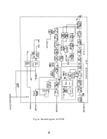
Страница 40: ...28 Fig 4 1 Block Diagram RF PCB...
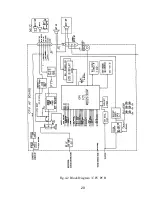
Страница 41: ...29 Fig 4 2 Block Diagram CPU PCB...
Страница 55: ...43 6 2 RAY210 ASSEMBLY DRAWING...
Страница 57: ...45 6 3 SCHEMATIC DIAGRAM Fig 6 1 Schematic diagram RF PCB...
Страница 58: ...46 Fig 6 2 Schematic diagram CPU PCB l...
Страница 59: ...47 Fig 6 2 Schematic diagram CPU PCB 2...
Страница 60: ...48 Fig 6 3 RF PCB Layout Top View...
Страница 61: ...49 Fig 6 4 RF PCB Layout Rear View...
Страница 62: ...50 Fig 6 5 CPU PCB Layout Top view...
Страница 63: ...51 Fig 6 5 CPU PCB Layout Rear View...
Страница 64: ...52...
Страница 75: ...63...


