background image

AVH-P5200BT/XNUC

104

1

2

3

4

1

2

3

4

C

D

F

A

B

E

Enlarged

RF

AGND2

Oscilloscope

The skew adjustment for the pickup is required when the following replacement is performed:
   (1) Replacement of the pickup unit
   (2) Replacement of the spindle motor
   (3) Replacement of the carriage chassis
   (4) Replacement of the main shaft of the pickup unit
   (5) Replacement of the sub-shaft of the pickup unit

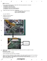
 • Measuring instrument, jigs and tools: Oscilloscope

Driver for adjusting SKEW => torques (T2) driver
Bond for fixing SKEW (GEM1033)
Bond for screw lock (GEM1068)

 • Disc used: GGV1018

 • Measurement criterion: AGND2
 • Measurement point: RF

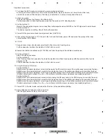
 • Connection diagram

 DVD core unit

-

SKEW adjustment

Symptoms seen in case of inadequate adjustment: Worsened error ratio 10-3 (normally 10-4 or less)
Large RF jitter
RF waveform is distorted
Tracking leading-in/servo is unstable

* Note: Do not directly look at laser beam in adjustment.

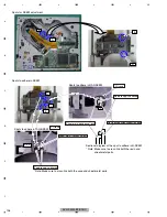
There are two types of adjustments available: adjustment while monitoring the RF waveform with the oscilloscope 
(method

1

) and adjustment while checking the RF level values with the OSD (method 

2

).

The adjustment procedure is shown below. For how to enter the test mode and the operation procedure, see the 
sections in the Service Test Mode.

Содержание Super Tuner IIID AVH-P5200BT

Страница 1: ... 04 01 Singapore 159936 PIONEER CORPORATION 2010 AVH P5200BT XNUC CRT4537 DVD AV RECEIVER AVH P5200BT XNUC AVH P5250BT XNRD AVH P5200DVD XNUC AVH P5250DVD XNRC AVH P5250DVD XNRD AVH P5250DVD XNRI This service manual should be used together with the following manual s Model No Order No Mech Module Remarks CX 3268 CRT4534 MS7 DVD Mech Module Circuit Descriptions Mech Descriptions Disassembly For det...

Страница 2: ...ive the laser diodes for DVD and CD respectively When Q1103 or Q1104 is shorted between their terminals the laser diodes for DVD or CD will radiate beam If the top cover is removed with no disc loaded while such short circuit is continued the naked eyes may be exposed to the laser beam CAUTION Where in a manufacturer s service documentation for example in circuit diagrams or lists of components a ...

Страница 3: ... 5 6 7 8 C D F A B E CAUTION Danger of explosion if battery is incorrectly replaced Replaced only with the same or equivalent type recommended by the manufacture Discord used batteries according to the manufacture s instructions ...

Страница 4: ...ide the product Please check that neither solder debris nor screws remain inside the product 8 There should be no semi broken wires scratches melting etc on the coating of the power cord Damaged power cords may lead to fire accidents so please be sure that there are no damages If you find a damaged power cord please exchange it with a suitable one 9 There should be no spark traces or similar marks...

Страница 5: ...ONITOR PCB ADJUSTMENT 110 9 EXPLODED VIEWS AND PARTS LIST 112 9 1 PACKING 112 9 2 EXTERIOR 1 114 9 3 EXTERIOR 2 116 9 4 EXTERIOR 3 118 9 5 EXTERIOR 4 120 9 6 DVD MECHANISM MODULE 124 10 SCHEMATIC DIAGRAM 126 10 1 DVD AMP UNIT ANALOG PART 126 10 2 DVD AMP UNIT SYSTEM PART GUIDE PAGE 128 10 3 DVD AMP UNIT POWER SUPPLY PART 134 10 4 DVD AMP UNIT MMD PART GUIDE PAGE 136 10 5 DVD AMP UNIT I F PART GUID...

Страница 6: ...egion code is reset to its initial value due to replacement of the DVD unit etc change the region code to that written on the name plate of the main unit Contact the PSN Division for the region changing procedure 9 Countermeasures to user complaints on iPhone iPod touch lip synchronization When a video is replayed the video and audio may be out of synchronization depending on the connected iPod or...

Страница 7: ...olders lead free solders have higher melting points by approximately 40 C Therefore for lead free soldering the tip temperature of a soldering iron must be set to around 373 C in general although the temperature depends on the heat capacity of the PC board on which reworking is required and the weight of the tip of the soldering iron Compared with eutectic solders lead free solders have higher bon...

Страница 8: ...ase Normal Reverse Bass boost Gain 12 dB to 0 dB DVD Player System DVD video Video CD CD WMA MP3 AAC DivX JPEG system Usable discs DVD video Video CD CD CD R RW DVD R RW RDL Region number 1 Frequency response 5 Hz to 44 000 Hz with DVD at sampling frequency 96 kHz Signal to noise ratio 96 dB 1 kHz IHF A net work RCA level Output level Video 1 0 Vp p 75 ohm 0 2 V Number of channels 2 stereo MP3 dec...

Страница 9: ...uner Frequency range 87 9 MHz to 107 9 MHz Usable sensitivity 9 dBf 0 8 μV 75 ohm mono S N 30 dB Signal to noise ratio 72 dB IHF A network AM tuner Frequency range 530 kHz to 1 710 kHz 10 kHz Usable sensitivity 25 μV S N 20 dB Signal to noise ratio 62 dB IHF A network Bluetooth AVH P5200BT Version Bluetooth 2 0 certified Output power 4 dBm Max Power class 2 CEA2006 Specifications Power output 14 W...

Страница 10: ...X JPEG system Usable discs DVD video Video CD CD CD R RW DVD R RW RDL Region number for Middle East Asian and South African models 2 for Southeast Asian models 3 Frequency response 5 Hz to 44 000 Hz with DVD at sampling frequency 96 kHz Signal to noise ratio 96 dB 1 kHz IEC A net work RCA level Output level Video 1 0 Vp p 75 ohm 0 2 V Number of channels 2 stereo MP3 decoding format MPEG 1 2 Audio ...

Страница 11: ...oding format Home Theater Ver 3 4 5 2 6 avi divx FM tuner Frequency range 87 5 MHz to 108 0 MHz Usable sensitivity 9 dBf 0 8 μV 75 ohm mono S N 30 dB Signal to noise ratio 72 dB IEC A network AM tuner Frequency range 531 kHz to 1 602 kHz 9 kHz 530 kHz to 1 640 kHz 10 kHz Usable sensitivity 25 μV S N 20 dB Signal to noise ratio 62 dB IEC A network Infrared remote control Wavelength 945 nm Output ty...

Страница 12: ...AAC DivX JPEG system Usable discs DVD video Video CD CD CD R RW DVD R RW RDL Frequency response 5 Hz to 44 000 Hz with DVD at sampling frequency 96 kHz Signal to noise ratio 96 dB 1 kHz IEC A net work RCA level Output level Video 1 0 Vp p 75 ohm 0 2 V Number of channels 2 stereo MP3 decoding format MPEG 1 2 Audio Layer 3 WMA decoding format Ver 7 7 1 8 9 10 11 2ch audio Windows Media Player AAC de...

Страница 13: ...sable sensitivity 9 dBf 0 8 μV 75 ohm mono S N 30 dB Signal to noise ratio 72 dB IEC A network AM tuner Frequency range 531 kHz to 1 602 kHz 9 kHz 530 kHz to 1 640 kHz 10 kHz Usable sensitivity 25 μV S N 20 dB Signal to noise ratio 62 dB IEC A network Bluetooth AVH P5250BT Version Bluetooth 2 0 certified Output power 4 dBm Max Power class 2 Infrared remote control Wavelength 945 nm Output typ 10 m...

Страница 14: ...gos are owned by the Bluetooth SIG Inc and any use of such marks by Pioneer Corporation is under license Other trademarks and trade names are those of their respective owners BT model only is a trademark of DVD Format Logo Licensing Corporation UC model only UC model only RC RD RI models RC RD RI models ...

Страница 15: ...F c RESET 6 TRACK d SD memory card slot 7 eject CAUTION Use an optional Pioneer USB cable CD U50E to connect the USB audio player USB mem ory as any device connected directly to the unit will protrude out from the unit and may be dangerous Do not use unauthorized products For details on how to operate a navigation unit from this unit refer to its operation manual Note When the navigation unit is c...

Страница 16: ...ss to select the tuner band when tuner is selected as a source Also used to cancel the control mode of functions Press to switch be tween modes when playing discs with compressed audio and audio data CD DA such as CD EXTRA and MIXED MODE CDs j MENU Press to display the DVD menu during DVD playback TOP MENU Press to return to the top menu during DVD playback k AUDIO Press to change the audio langua...

Страница 17: ...d separately Microphone input Jack MIC AVH 5200BT only 17 cm 6 3 4 in 17 cm 6 3 4 in Navigation unit AVIC U220 sold separately Antenna input Tuner box supplied Antenna cable supplied 80 cm 2 ft 7 in IP BUS cable Pioneer IP BUS accessories Connection method 1 Clamp the lead 2 Clamp firmly with needle nosed pliers Note The position of the parking brake switch depends on the vehicle model For details...

Страница 18: ...o rear view image when the gear shift is moved to REVERSE R WARNING USE INPUT ONLY FOR REVERSE OR MIRROR IMAGE REAR VIEW CAMERA OTHER USE MAY RESULT IN INJURY OR DAMAGE CAUTION The screen image may appear reversed The rear view camera function is to be used as an aid for backing into a tight parking spot Do not use this function for entertainment purposes Objects in the rear view may appear closer...

Страница 19: ...1 8 in It is necessary to change AV Input in System Menu when connecting the external video component When using a display connected to rear video output This product s rear video output and rear audio output are for connection of a display to enable passengers in the rear seats to watch the DVD etc WARNING Never install the display in a location where it is visible to the driver while driving Con...

Страница 20: ... wired remote control adaptor can be connected sold separately Microphone input Jack MIC AVH 5250BT only 17 cm 17 cm Antenna input Tuner box supplied Antenna cable supplied 80 cm 80 cm IP BUS cable Pioneer IP BUS accessories Connection method 1 Clamp the lead 2 Clamp firmly with needle nosed pliers Note The position of the parking brake switch depends on the vehicle model For details consult the v...

Страница 21: ...od When connecting with a rear view camera When this product is used with a rear view camera it is possible to automatically switch from the video to rear view image when the gear shift is moved to REVERSE R WARNING USE INPUT ONLY FOR REVERSE OR MIRROR IMAGE REAR VIEW CAMERA OTHER USE MAY RESULT IN INJURY OR DAMAGE CAUTION The screen image may appear reversed The rear view camera function is to be...

Страница 22: ...raffic accident Fix the optical cable connection box securely with the hook and loop fastener or lock tie If the unit is loose it disturbs driving stability which may result in a traffic accident CAUTION Install this unit using only the parts supplied with this unit If other parts are used this unit may be damaged or could dismount itself which leads to an accident or other problems Do not install...

Страница 23: ...necessary to change AV Input in System Menu when connecting the external video component When using a display connected to rear video output This product s rear video output and rear audio output are for connection of a display to enable passengers in the rear seats to watch the DVD etc WARNING Never install the display in a location where it is visible to the driver while driving Connecting the s...

Страница 24: ...splay video audio and operations must be normal 5 CD Play back a CD Track search Display audio and operations must be normal 6 FM AM tuner Check FM AM tuner action Seek Preset Switch band to check both FM and AM Display audio and operations must be normal If the reception sensitivity is poorer than normal the gasket on the FM AM tuner unit may be damaged or lost 7 Check whether no disc is inside t...

Страница 25: ...Service Main PCB Unit H F G K BT ANT PCB J Tuner Box Unit B A BT PCB I M Keyboard PCB Volume PCB Unit C D E DVD Core Unit MS7 Compound Unit A Compound Unit B BT Model DVD Model L Switch PCB Unit Monitor PCB Panel PCB DVD Amp Unit Main PCB Unit H F G K A M Keyboard PCB Volume PCB Unit L Switch PCB Unit ...

Страница 26: ...B Unit Number CWN3130 I C D E Unit Name Tuner BOX Unit Keyboard Unit Consists of Panel PCB Keyboard PCB Unit Number CWN4996 Unit Name Keyboard Unit Monitor Unit Service Consists of Monitor PCB BT PCB BT ANT PCB Unit Number CXX2841 H I Unit Name Monitor Unit Service Unit Number CWN4992 B C D E Unit Name Monitor Unit Unit Number EWM5101 Unit Name Main PCB Unit Unit Number Unit Name Switch PCB Unit U...

Страница 27: ...t 20P FFC GGD1209 Drive Unit 40P 20P Extension Board 40P 20P Extension Board GGF1461 Mother Unit Only 20P side is used Name Jig No Remarks Grease GEM1038 DVD Mechanism Module Grease GEM1045 DVD Mechanism Module Grease GEM1050 DVD Mechanism Module Grease GEM1085 DVD Mechanism Module Grease GEM1024 DVD Mechanism Module and Drive Unit Grease GEM1043 DVD Mechanism Module and Drive Unit Locking agents ...

Страница 28: ...hipping out the product be sure to clean the following portions by using the prescribed cleaning tools Portions to be cleaned Cleaning tools DVD pickup lenses Cleaning liquid GEM1004 Cleaning paper GED 008 Portions to be cleaned Cleaning tools Fans Cleaning paper GED 008 ...

Страница 29: ...AVH P5200BT XNUC 29 5 6 7 8 5 6 7 8 C D F A B E ...

Страница 30: ...AGND 1 2 3 4 5 CKS6008 A CN5002 PWRVI 1 PWRVI 2 PWRVI 3 NC 4 GNDD 5 GNDD 6 GNDD 7 PWGR 8 ADVY 9 ADVX 10 PLXV 11 PLYV 12 ILR 13 ILG 14 ILB 15 GNDKEY 16 GNDKEY 17 NC 18 NC 19 KEY1 20 NC 21 GNDILM 22 NC 23 ILMB 24 NC 25 DtoG 26 GtoD 27 DGCLK 28 StoG 29 GtoS 30 GRST 31 VGND 32 ANAG 33 ANAR 34 CSYNC 35 ANAB 36 VGND 37 MOVBS 38 GNDBL 39 GNDBL 40 GNDBL 41 NC 42 PWRBL 43 PWRBL 44 PWRBL 45 BLERR1 46 BLCLK ...

Страница 31: ...8 VD 29 VD 30 VD CKS3878 A CN795 BT_MIC1P SYS B BT_MIC1N BT_RST BT_SPK1P BT33 BT_SPK1N S_BTTX GNDBT BT_SRX 1 2 3 4 5 6 7 8 9 10 CKS4822 A CN1741 1 GND 2 FUN CKS5858 A CN561 REMIN VCC33 NC AUX_L AUX_AGND AUX_R AUX_V AUX_VGND USB USB USB_GND USB_GND USB_5V ILM B DSENS ROT_IN2 ROT_IN1 ILMGND LED_B LED_G LED_R RESET GNDKEY KDT1 KDT0 USB_5V 1 2 3 4 5 6 7 8 9 10 11 12 13 14 15 16 17 18 19 20 21 22 23 24...

Страница 32: ...CIN AVSCK 18 68 AVSDATA STANBY 67 90 EVSDA 101 EVSCK 102 EVSEL 103 WIRED 160 WIREDAD 161 REARMUTE AMPMUTE 128 129 AMPPW ASENS 131 21 6 TUNCE2 TUNCE2 19 TUNCE 11 TUNCK 13 TUNDI 15 TUNDO S_TTUN T_STUN HSLK RDSLK RDT RCK 5 RDSHSLK ARET3 TUNCE2 TUNSL TUNCE TUNCK TUNSL TUNCE TUNCK S_TTUN T_STUN HSLK RDSLK RDT RCK Q781 1 RDSLOCK Q782 7 RDSDATA Q781 Q542 Q544 3 RDSCK MS_to_S 44 S_to_MS 43 IRQPW 111 XRST ...

Страница 33: ...EVCLK EVSTB SYSMUTE ASENS 101 EVSCK 102 EVSEL 103 WIRED 160 WIREDAD 161 BTMIC_GND BTMIC_IN BTMIC_GND BTMIC_IN 7 9 D153 Q153 2 2 1 2 Q153 1 2 Q401 RCA_RL RCAMUTE 1 2 Q442 RCA_FL 2 2 Q442 RCA_SWL 2 2 Q441 Q161 Q163 Q162 REARMUTE AMPMUTE 128 129 AMPPW ASENS 131 21 P B PBSENS Q123 9 1 2 PBSENS 146 BSENS Q122 Q125 BSENS PBSENS 2 2 BSENS 20 MUTE TELMUTE Q123 14 2 2 TELMUTEIN 145 ILM ISENS Q121 13 ISENS ...

Страница 34: ...TSW 25 24 StoG S_to_G 98 GRST 24 G_to_D 25 D_to_G 23 DGCLK 38 ILR 37 ILG 36 ILB 43 PWGR LEDR1 LEDG1 LEDB1 GRST 99 21 GtoS G_to_S 97 ILMLD 53 ILMDT MVIPW 54 155 REMIN 7 ROTIN1 63 ROTIN2 ROTIN1 ROTIN2 62 RESET 16 DSENS 176 KDT0 175 KDT1 X1 X2 174 14 15 ILMCK 55 AUX S3002 RESET MUTE VOLUME DSENS 25 S3001 S3003 DSENS KDT0 15 ROT_IN2 24 ROT_IN1 23 S3004 EJECT KDT1 LED_R LED_G LED_B VCC33 ILM B REMIN AU...

Страница 35: ...C 14 64 MC SCKDAC 15 62 71 SDODAC SCKDAC LTDAC SOAMUTE D_TRCCLK ML LTDAC SYS B ADAC IC941 PCM1753DBQ Q942 1 2 Q941 1 2 CPRST CPDT CPCK VCC VCC 61 nRESET I2C_SDA I2C_SCL CPRST 46 CPSDL 47 4 13 12 5 CPSCK 53 G_to_D 54 D_to_G 55 DGCLK DGCLK 1 2 Q951 2 2 Q951 MDQ 0 15 MA 0 11 A 0 9 D 0 15 D TRCD 0 3 A 0 9 D 0 15 A 0 9 D 0 15 IC923 TC74LCX16373FT LATCH A 0 9 D 0 15 IC522 TC7MBL6126SFK USB BUFFER A1 L52...

Страница 36: ...DQM1 17 188 NCAS XRAS 18 189 NRAS XCSM 190 NCSM 20 193 BA0 21 197 BA1 BA0 BA1 15 179 DQM0 39 19 20 27 39 53 37 33 35 12 10 180 DQM1 LDQM UDQM MCK VHALF TD FD MD CONT1 CONT2 DRV2 DRV3 FOP 183 MCK 185 121 MCKI VDSENS CAS RAS WE BD8217EFV IC1201 MOTOR DRIVER CTL1 CTL2 FG FCO FIN VC TIN LDIN SPIN HALL_VC V_OUT 41 LDO 42 LDO CN1201 5 6 HALL_BIAS HBM HALL_BIAS COIL_V 127 126 66 71 54 53 FG CONT2 CONT1 H...

Страница 37: ...VCC5 REG VCC5 VD8 5 4 3 VIN VOUT ON OFF S 1133B50 U5 IC1901 VCC5 REG A 7 B C D FE1 FE2 78MD CDMPD 65MD DVDMPD TEMP TH RF 1 2 4 3 F F FOM FOP TOP TOM T T VD8 XRESET NRES 501 MHz ANALOG LOUT CN1901 9 3 17 25 11 10 13 8 7 12 1 2 19 VREF COMPOSIT COMPOSITE STANBY STANDBY HSTCMD CMDCOMN SLVSTS STSCOMN IRQPWR AMUTE IECOUT 1 3 VCC33 VDD5 NJM2885DL1 33 IC1004 3 3V REG IN OUT 2 8 VDD5 VCC12 IC1005 1 2V REG...

Страница 38: ...S MONVBS AV0INB 38 31 30 29 28 27 26 52 133 NRST GERDA L MN103SH13UB IC5502 H TOUCH PANEL 1 ADVY 9 ADVY 8 ADVX 7 ADVX 6 PLXV 5 PLXV 4 PLYV 3 PLYV 2 CN2021 A DO 3 68 GPI014 DI 2 69 GPI013 SK 1 70 GPI012 CS EEPROM IC5501 S 93C66BD0I I8 IC5312 TC7SET08FUS1 1 2 3 OUT IN IC5311 TC75S57FU 4 8 10 2 INA OUTY IC5702 TC7SET08FUS1 1 4 VOUT VIN IC5301 NJM2505AF C VIDEO DtoG GRST 41 38 142 145 DV0R5 DV0R4 SDAT...

Страница 39: ...ER CN3500 G 1 2 LED4 LED4 FAULT SW CLKI DIM 15 IC5701 TK61222CQ6 4 8 10 2 INA OUTY IC5702 C7SET08FUS1 3 1 CN5502 CN5601 CN5701 CN5802 1 GD33V GD33V 2 4 GRST1 5 TRCST 6 TRCCLK 8 SDATA 9 SCLOCK DCLK SHUT HSYNC VSYNC LHSY LVSY 11 14 5 8 6 4 7 1 LED3 LED3 17 2 LED2 LED2 18 3 LED1 LEDR1 5 LEDG1 6 LEDB1 3 KEY1 1 ILMB LED1 19 4 TEMP1 9 TRCD 0 3 18 23 LR 0 5 25 30 LG 0 5 32 37 39 16 14 13 LB 0 5 Q5701 Q57...

Страница 40: ...VD5 H VD8 H DDCCLK Clock Out Starts Communication with Display microcomputor Source Keys operartive Source ON SYSPW H Standby BSENS Pin20 ASENS Pin21 ASENBO Pin35 DDCCLK Pin92 VD5 8 Pin113 114 SYSPW Pin130 Y Y STANBY H STANBY Pin90 Y Frequency of 370 kHz SOCSTBY H SOCSTBY Pin91 Y VDD Pin11 DSENS 1 15 V to 1 95 V DSENS Pin176 Y ...

Страница 41: ... Within prescribed value Lens cleaning completed Clean lens Check measured value of error ratio Check error ratio Within prescribed value Replace pickup To Replace pickup To Replace pickup To Replace pickup Check 2 Check 3 Yes Yes Yes Yes Yes Yes No No No No No Make sure to avoid any unwiped spots or actuator breakage Make sure to avoid any unwiped spots or actuator breakage Judgement of pickup co...

Страница 42: ...en terminals in the focus closed status in the test mode Mind breakage of a laser diode caused by static electricity Remarks LD current value ref GGV1025 DVDLD1 VCC5_3 60 390 mV 10 65 mA NO 1 Disc used Spot to check Rated value Remarks LD current value ref TCD 782 CDLD1 VCC5_3 60 360 mV 10 60 mA NO 2 Disc used Spot to check Rated value ...

Страница 43: ...or ratio of a specified ID in the tracking closed status in the test mode TCD 782 ASMAX value on test mode screen 0000 0029 or more check RF level requiring gain 6dBup ASMAX level Remarks GGV1025 ASMAX value on test mode screen 0000 0026 or more check RF level requiring gain 6dBup ASMAX level NO 1 2 Disc used Spot to check Rated value GGV1025 ID 200000 1 000E 3 or less Remarks GGV1025 ID 40000 1 0...

Страница 44: ...s operation take time YES YES 1 When a flash ROM generally needs to be replaced by service do not replace an IC but a core unit as no key or others is written in a flash alone Flash life OK Execute check 12 AVCC5 voltage OK Execute check 8 AVCC5 voltage OK Execute check 8 Video circuit OK Execute check 11 DACCLK normal Execute check 9 SDRAM IF OK Execute check 6 STANBY OK Execute check 1 VD8 VCC5 ...

Страница 45: ...k Check the voltage of the sending pin when the power is ON Checking should be based on DGND PCB side A Fig 1 1 Spots to check in STANDBY STANDBY DGND1 Check 1 STANBY OK NO Spot to check Module NO Rated value Unit 1 STANDBY DGND1 ALL VCC33 0 6V or more V ...

Страница 46: ...ck in VDD5 VCC33 VCC12 voltages IC1401 FLASH power Data IC1402 FLASH power Program IC1480 SDRAM power IC1501 DVD LSI power IC1501 DVD LSI power IC1004 and IC1005 DC DC converter VCC 3 3V 1 2V output F E driver control system DGND1 VCC33_1 VDD5_2 VCC12 1 Check 2 VDD5 VCC33 VCC12 Power supply voltage OK NO Spot to check Module NO Rated value Unit 1 VDD5_2 DGND1 ALL 5 0 0 4 V 2 VCC33_1 DGND1 ALL 3 3 ...

Страница 47: ...Check Check the voltage of the sending pin when the power is ON Checking should be based on DGND PCB side A Fig 3 1 Spots to check in RESET DGND1 NRES Check 3 RESET OK NO Spot to check Module NO Rated value Unit 1 NRES DGND1 ALL VCC33 x 0 7 or more V ...

Страница 48: ...heck the voltage of the sending pin when the power is ON Checking should be based on DGND PCB side A Fig 4 2 Spots to check in VSENS IC1501 DVD LSI IC1004 DC DC converter VSENS DGND1 IC1005 regulator R1550 R1551 voltage dividing circuits Check 4 VSENS OK VCC33 NO Spot to check Module NO Rated value Unit 1 VSENS DGND1 ALL VCC33 x 0 7 or more V ...

Страница 49: ... when the power is ON If NG is found check the relevant lines periphery of IC1501 soldering of peripheral components and defective components GND Fig 5 2 Rated value of a clock PCB side A Fig 5 3 Spots to check in 27 MHz IC1501 DVD LSI X1501 27 MHz Crystal VCC12 VCC33 Rated value DGND1 IC1501 156pin Check 5 27 MHz normal NO Spot to check Module NO Rated value Unit 1 IC1501 156pin ALL 27 MHz 50ppm ...

Страница 50: ...C1480 33pin IC1501 198pin 56 ohm 5 10 MA9 IC1480 34pin IC1501 194pin 56 ohm 5 11 MA10 IC1480 22pin IC1501 199pin 56 ohm 5 12 MA11 IC1480 35pin IC1501 192pin 56 ohm 5 13 MDQ0 IC1480 2pin IC1501 160pin 56 ohm 5 14 MDQ1 IC1480 4pin IC1501 162pin 56 ohm 5 15 MDQ2 IC1480 5pin IC1501 164pin 56 ohm 5 16 MDQ3 IC1480 7pin IC1501 168pin 56 ohm 5 17 MDQ4 IC1480 8pin IC1501 170pin 56 ohm 5 18 MDQ5 IC1480 10pi...

Страница 51: ...AVH P5200BT XNUC 51 5 6 7 8 5 6 7 8 C D F A B E PCB side B Spot to check 1 IC1480 PCB side A Spot to check 2 IC1501 Fig 6 2 Spots to check in SDRAM I F ...

Страница 52: ... power is ON Checking should be based on PGND AGND PCB side A Fig 7 2 Spots to check in VD8 VCC5 voltages F E driver system PU power IC1901 VCC 5V REG IC VD8_1 PGND3 VCC5_1 AGND1 VD Check 7 VD8 VCC5 Power supply voltage OK NO Spot to check Module NO Rated value Unit 1 VD8_1 PGND3 ALL 8 0 0 4 V 2 VD PGND_3 ALL 8 0 0 4 V 3 VCC5_1 AGND1 ALL 5 0 0 1 V ...

Страница 53: ...LE1 to check the voltage of the sending pin Checking should be based on PGND AGND PCB side A Fig 8 2 Spots to check in VD8 AVCC5 voltages IC1801 Audio DAC IC1900 AVCC 5V REG IC GNDAU1 AVCC5 VD PGND3 Check 8 AVCC5 voltage OK NO Spot to check Module NO Rated value Unit 1 VD PGND_3 ALL 8 0 0 4 V 2 AVCC5 GNDAU1 ALL 5 0 0 1 V ...

Страница 54: ...should be based on DGND If NG is found check the relevant lines periphery of IC1501 soldering of peripheral components and defective components GND Fig 9 2 Rated value of a clock IC1501 DVD LSI X1501 27 MHz Crystal IC1801 Audio DAC VCC12 VCC33 Rated value 1 Rated value 2 Rated value 3 Check 9 DACCLK normal NO Spot to check 1 sending pin Media Rated value 1 Rated value 2 Rated value 3 1 DACCK DVD 2...

Страница 55: ...AVH P5200BT XNUC 55 5 6 7 8 5 6 7 8 C D F A B E PCB side A Spot to check 2 IC1501 148pin Spot to check 1 probe Fig 9 3 Spots to check in 27 MHz DACCLK ...

Страница 56: ...RO SRCK GNDAU IECOUT Fig 10 1 Audio circuit How to check Play back DVD REF A1 TITLE2 CHAPTER1 48k 16bit 1kHz 0dB Checking should be based on DGND If NG is found check the relevant lines periphery of main components described above soldering of peripheral components and defective components GND Fig 10 2 Rated value of serial three wires IC1801 Audio DAC IC1501 DVD LSI Rated value 1 Rated value 2 Ch...

Страница 57: ...following check based on GNDAU2 using the measurement circuit shown below Fig 10 4 Rated value of analog audio out LO RO Rated value is an effective value rms ADOUT SRCK LRCK 47 k 47 k LO RO GNDAU2 NO Spot to check 1 sending pin Rated value rms Reference waveform 4 LO 1400 150 mV Waveform 4 5 RO 1400 150 mV Waveform 4 ...

Страница 58: ...ould be based on DGND Checking should be performed after connecting 24Pin FFC to the jig or other equipment PCB side A Fig 10 6 Spot to check in digital audio signal IECOUT LO RO GNDAU IEC NO Spot to check 1 sending pin Rated value 1 Rated value 2 Reference waveform 6 IEC VCC33V 0 6V or more 0 4V or less Waveform 5 ...

Страница 59: ... and Trigger line to TV trigger and line 150 respectively If NG is found check the relevant lines periphery of main components described above soldering of peripheral components and defective components PEAK Rated value COMPOSITE signal Color burst Pedestal level BOTTOM Horizontal synchronous signal Fig 11 2 Waveform when 100 composite white is output IC1501 DVD_LSI Video DAC COMPOSITE Check 11 Vi...

Страница 60: ...tion is heavy the FLASH memory may have reached the end of its life Whether the FLASH memory has reached the end of its life is determined by viewing the display of the LD live time 1 Display the LD live time For how to display the LD live time see FE Test Mode 2 The second digit of the live time from the left being E as in E means the FLASH memory has reached the end of its life E g ...

Страница 61: ...sec div Reference voltage DGND2 CH1 IECOUT CH1 SRCK Reference voltage DGND2 1 V div 5 usec div 1 V div 500 nsec div Reference voltage DGND2 CH1 LRCK 1 V div 5 usec div Reference voltage DGND2 Waveform 3 Waveform 2 Waveform 1 Waveform 5 Waveform 4 G G G G G G WHITE 100IRE CH1 COMPOSITE 200 mV div 10 usec div Reference voltage GNDV1 Waveform 6 ...

Страница 62: ...2 A0 A0h REQUEST error X X X X Issuance of read ERROR 02 A1 A1h Issuance of read command failed X X X X command failed chip dependent L0 adjustment NG ERROR 02 A2 A2h L0 adjustment NG X X X X L1 adjustment NG ERROR 02 A3 A3h L1 adjustment NG X X X X LD system NG ERROR 02 A4 A4h LD system NG X X X X Gain adjustment system ERROR 02 A5 A5h Gain adjustment system NG X X X X NG Gain determination ERROR...

Страница 63: ... Content Protection for Recordable Media Copyright technology for the digital contents used for recordable DVDs or memory cards 8 Available only for the models compatible with DVD VR 9 This occurs when the audio property information notice is sent from the DVD mecha but no audio property activation notice is returned The time taken for occurrence should be specified in the latency time for the aud...

Страница 64: ...AVH P5200BT XNUC 64 1 2 3 4 1 2 3 4 C D F A B E ...

Страница 65: ...AVH P5200BT XNUC 65 5 6 7 8 5 6 7 8 C D F A B E ...

Страница 66: ...T 7 REAR MONITOR OUTPUT 8 VIDEO INPUT 1 FL 2 RL 3 FL 4 RL 5 FR 6 RR 7 FR 8 RR 9 P B 10 BGSENS 11 ACC 12 B REM 13 ILM 14 MUTE 15 B UP 16 GND 16 15 2 1 1 2 5 6 1 SUBWOOFER OUTPUT R 2 SYBWOOFER OUTPUT L 3 REAR OUTPUT R 4 REAR OUTPUT L 5 FRONT OUTPUT R 6 FRONT OUTPUT L 11 10 9 8 7 6 5 4 3 2 1 IP BUS INPUT 1 BUS 2 BUSG 3 BUSLG 4 NC 5 BUS 6 BUSRG 7 BUSL 8 ASENBO 9 BUSR 10 BUSR 11 BUSL 1 CCR 2 CCG 3 CCB ...

Страница 67: ...FE test mode image Continue to EDC1 test mode image Continue to EDC2 test mode image Select LD live time mode Continue to LD live time mode image Select simplified FE test mode Continue to simplified FE test mode Test mode image Key operation Operation status Contents displayed by the DVD mecha only those compatible with video Eight letters worth of the data is transmitted to the product to the HO...

Страница 68: ...IN3 offset cancel value VIN4 offset cancel value VIN5 offset cancel value VIN6 offset cancel value VIN7 offset cancel value VIN8 offset cancel value VIN9 offset cancel value VIN10 offset cancel value Power ON F close F search 1A00 0000 Focus closed status FEMAX level FEMIN level ASMAX level ENVMAX level FE normalization coefficient Spindle gain coefficient TEMAX level display TEMIN level display C...

Страница 69: ...f track adjustment result Tracking close Focus Jump L0 layer 2000 0000 L1 layer 2100 0000 CRG Operated while keys are pressed down 2B00 0000 CRG 2C00 0000 CRG Power_OFF CRG Power_OFF Operated while keys are pressed down 3B00 0000 CRG 3C00 0000 CRG 2x00 0000 2FFF 0000 3000 0000 3FFF 0000 FBAL coefficient 0 layer FBAL coefficient 1 layer Focus gain coefficient 0 layer Focus gain coefficient 1 layer ...

Страница 70: ...er 8 L1 layer Note The equipment needs to be powered OFF and activated again in the test mode as no restoration is possible in case of an error in the Power_OFF Tracking closed status Measure error ratio FBAL coefficient 0 layer FBAL coefficient 1 layer Focus gain coefficient 0 layer Focus gain coefficient 1 layer Tracking gain coefficient 0 layer Tracking gain coefficient 1 layer AS normalization...

Страница 71: ...is selected or ejected 1 4 EDC 1 2 test mode 0000 0000 Select 0 layer Select 1 layer Specify ID Start EDC 1 2 0000 0000 0100 0000 1003 0000 1103 0000 0 layer 10 1 layer 11 Note is the ID specified value 0 layer 20 1 layer 21 Note is the current ID value EJECT operation Test mode Eject Note is the current ID value EDC test mode image Legend Key operation Operation status Contents displayed by the D...

Страница 72: ...000 0000 Display CD LD live time Display DVD LD live time Set CD LD live time 10 Note represents CD LD live time 20 Note represents DVD LD live time Specify the set time 30 Note is the set time Register the set time Set DVD LD live time Specify the set time 40 Note is the set time Register the set time 6 5 2 1 1 4 1 4 5 5 8 8 10 Note represents CD LD live time 20 Note represents DVD LD live time L...

Страница 73: ... DVD Outer Middle DVD Middle CD CD Select Display error ratio CRG Move completed In case of an error In case of an error in Power_OFF Select CRG transfers to the outermost circumference Screen transition Simplified FE test mode Numbers on each screen can be selected with the test key commands No display data for the test mode is notified in the simplified FE test mode Notes The simplified FE test ...

Страница 74: ...ervice test mode is enabled only when the test mode is activated At this time no normal operation is executed 2 No request from the host is received while the core executes the test mode command 3 The core start up notice is not necessary in the test mode 3 Requests for HOST The service test mode requires two items the item that displays the notice command in the FE test mode in HOST and the item ...

Страница 75: ...coefficient 1 3 05h ENV offset coefficient 1 4 06h TG offset coefficient 1 5 07h DBAL coefficient 1 6 30h VIN1 offset cancel value 1 7 31h VIN2 offset cancel value 1 8 32h VIN3 offset cancel value 1 9 33h VIN4 offset cancel value 1 10 34h VIN5 offset cancel value 1 11 35h VIN6 offset cancel value 1 12 36h VIN7 offset cancel value 1 13 37h VIN8 offset cancel value 1 14 38h VIN9 offset cancel value ...

Страница 76: ...aying RF level value End displaying RF level value Specify No of tracks Note 3 CRG CRG To simplified FE test mode To FE test mode Note 1 A media type is specified here Settings should be implemented according to this specification Note 2 Switching gains should be normal gain OEIC H OEIC H and FEPx4 amps ON Note 3 Any other operation is prohibited during measurement Note 4 Playback speed should be ...

Страница 77: ... LD live time mode 1 2 5 6 Display CD LD live time Display DVD LD live time Set CD LD live time Set DVD LD live time Specify set time Specify set time Register set time Register set time EDC1 mode 1 4 1 4 5 5 8 8 How to specify a set time Specify a digit with the commands 1 and 2 Commands 3 and 4 are to increase decrease the number Determine with the command 5 Cancel with the command 8 ...

Страница 78: ...N Choose Version Check among the monitor test mode menu screen Display specifications Operation specification Operational description Remote controller key Selection cursor up movement 2 Selection cursor down movement 8 Menu enter 5 1 Version Check Operation specification Operational description Remote controller key Return to test mode menu 1 Page up 9 Page down 7 When 8 digits of read number is ...

Страница 79: ...the adjustment complete mark to go out Outermost circumference inspection In case the outermost circumference inspection has never been performed In case the EEPROM initialization has been performed In case the adjustment value has been initialized Calibration inspection In case the calibration inspection has never been performed In case the EEPROM initialization has been performed In case the adj...

Страница 80: ...tion to the EEPROM then NG is displayed 1 Adjustment information Adjustment NG 1 byte The initial value and the setting value allowable range are as follows Before initial value After initial value Outermost value Outermost value Xmin 3Bh Xmin 78h Ymin 40h Ymin 78h Xmax F7h Xmax B4h Ymax F2h Ymax B4h A D correction value A D correction value X 33h X 00h Y 38h Y 00h Setting value allowable range X ...

Страница 81: ...ng information for the 16 points and the normal ending information total of 17 byte data are written into the EEPROM and the screen returns to the TOP menu Display specifications 16 points adjustment in process Order of display of the locations to be pressed This point is intended to end the calibration inspection and therefore the corrected value of this point is not obtained Operation specificat...

Страница 82: ...Factory are the corrected values in the Factory region and the values under User are the corrected values in the User region Sampling A D value X direction Y direction of the pressed point is displayed AD Value The coordinate X direction Y direction of the A D value of the pressed point corrected by the reference value for A D correction is displayed Normalization The coordinate X direction Y dire...

Страница 83: ...ill delete the cursor and another cursor will be displayed The incorrect touch will make the characters of cursor turn red Repeat this for 4 points and OK is displayed upon the last press of 4th point Display specifications The pushing order confirming Operation specification Operational description Remote controller key Return to top menu 1 ...

Страница 84: ...hting conditions are not applicable When the adjusted value has been initialized Data initialize When the EEPROM has been initialized Calibration inspection When the above mentioned lighting conditions are not applicable When the adjusted value has been initialized Data initialize When the EEPROM has been initialized User outermost circumference inspection When the above mentioned lighting conditi...

Страница 85: ... specifications Default of a cursor is the location of No Choose YES and decide initialize a setting value Don t turn off power while initializing When normally ends success is displayed When will not end in four seconds judged to be abnormal failure is displayed Operation specification Operational description Remote controller key Selection cursor left movement 4 Selection cursor right movement 6...

Страница 86: ...B RGB is plotted in the following pattern R100 R50 G100 G50 B100 B50 BLACK GRAY WHITE GREEN and MAGENTA dot signal The display of the screen will be changed in 1 second Operation specification Operational description Remote controller key Stop Restart 5 Return to test mode menu 1 MONOCHROME STRIPE Display of monochrome stripe signal 1dot Width Operation specification Operational description Remote...

Страница 87: ...STER SIGNAL Display of signal for step confirmation Operation specification Operational description Remote controller key Next signal 5 Return to test mode menu 1 CONTRAST Display of Black White signal Operation specification Operational description Remote controller key Next signal 5 Return to test mode menu 1 CENTER MARKER Display of signal for screen central location setting Operation specifica...

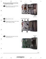
Страница 88: ...sconnect the connector 1 4 2 3 1 2 1 2 4 4 3 Grille Assy Holder Removing the Grille Assy Fig 1 How to assemble Grille Unit Fig 1 Slide the grille forward by pushing two tabs with tweezers or other item As the mother unit SD part is fixed with the grille insert it horizontally Attach and remove the grille unit by sliding it horizontally ...

Страница 89: ...6 7 8 C D F A B E Remove the seven screws and then sepa rate the Drive Unit and the Chassis Assy 1 1 1 1 1 1 1 1 Chassis Assy Drive Unit Left Side Rear Side Right Side How to separate the Drive Unit and the Chassis Assy Fig 2 Fig 2 ...

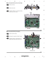
Страница 90: ...ift the Bracket toward the Drive Unit Remove the four screws Disconnect the connector and then remove the DVD Mechanism Module Disconnect the two connectors and then remove the Drive Unit 1 2 3 4 Removing the DVD Mechanism Module and the Drive Unit Fig 3 Bracket DVD Mechanism Module Drive Unit Drive Unit 4 ...

Страница 91: ...traighten the tabs at two locations indicated and then remove the Holder Remove the three screws Disconnect the connector Only BT model Straighten the tabs at three locations indi cated and then remove the DVD Amp Unit 1 2 3 1 2 3 Removing the Holder and the Panel Fig 4 Removing the DVD Amp Unit Fig 5 Panel Holder DVD Amp Unit ...

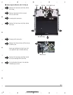
Страница 92: ...move the Spring Remove the screw and then remove the Arm and Cover Disconnect the connector Remove the five screws and then remove the Cover Disconnect the connector Remove the three screws and then remove the Motor Unit Removing the Motor Unit the Drive Unit can operate to lead to the Monitor Assy 1 2 3 Removing the Monitor Unit 1 2 Fig 6 Monitor Assy Motor Unit Arm and Cover 3 Cover 1 Spring 4 4...

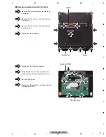
Страница 93: ...he Cover Remove the four screws and then remove the Case Unit Disconnect the connector Disconnect the three connectors Straighten the tabs at two locations indi cated and then remove the Monitor Unit Remove the screw Disconnect the connector and then remove the Keyboard PCB 1 2 3 4 5 6 7 8 Removing the Monitor Unit 2 2 Fig 7 Holder Case Unit Cover Keyboard PCB Monitor Unit ...

Страница 94: ...3 4 1 2 3 4 C D F A B E LCD plate Insert the tweezers thin one as shown in the figure and remove the tab Caution If you pick up the tab forcibly the plate bends It can be removed by just inserting the tweezers straightly Fig 7 ...

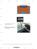
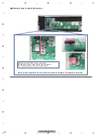
Страница 95: ...e sure to use jig GGF1539 If the antenna cable is directly unplugged without using jig GGF1539 you might damage your fingertip or fingernail How to Remove the Coaxial Jumper When unplugging Coaxial Jumper hook the point of jig GGF1539 on the lid of Coaxial Jumper and vertically draw out along with the engagement axis of connector How to Attach the Coaxial Jumper For inserting Coaxial Jumper adjust...

Страница 96: ...l the Cushion Align the cushion to PCB silk print and stick it Be careful not to touch the cushion to the USB terminal The sticking direction is shown on the right figure When you install the grille to the unit confirm the cushion is sticking on the keyboard unit properly ...

Страница 97: ...frame and the upper frame 3 Do not hold the front part of the upper frame because the intensity is low 4 Do not touch the switch on the ceiling surface of the mechanism Fig 1 5 Take care not to catch the flexible part on the side face 6 Take note that a deformation may be generated if you hold the front part of the upper frame or CRG mechanism part or a foreign object is inserted ...

Страница 98: ...AVH P5200BT XNUC 98 1 2 3 4 1 2 3 4 C D F A B E Do not touch here Handling NG Do not touch here Do not touch here Do not touch here Fig 1 ...

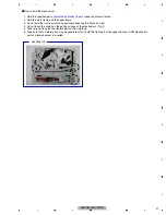
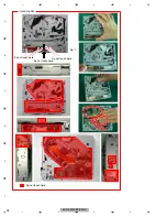
Страница 99: ... Set the ceiling surface of the mechanism module downward 3 Short circuit two parts of lands of the pickup flexible part Fig 1 4 Remove the connector of the pickup flexible part Fig 2 The flexible part is damaged if the board is removed without removing the flexible part so be sure to remove it 1 Unscrew two screws and remove the CRG motor ASS Y Fig 3 Locking screw CRG Locking screw CRG CRG motor ...

Страница 100: ...t 4 While holding up the tip of the pickup rack slide the main shaft and remove the PU unit Caution When you attach the PU again carry out the adjustment surely following the description in the service manual of the mounted product Be sure to carry out the actual applying of main shaft holddown spring PU unit Sub shaft Main shaft Fig 4 Actual applying Temporary applying Temporary applying part of ...

Страница 101: ...ouch the radiator Do not touch the ACT object lens Do not pull the FPC Do not touch the Miller or Collimator lens How to hold PU Fig 5 1 When you hold PU hold Handling OK part shown in the figure and do not hold Handling NG part Fig 5 Handling OK Handling NG ...

Страница 102: ...AVH P5200BT XNUC 102 1 2 3 4 1 2 3 4 C D F A B E ...

Страница 103: ...oscilloscope to the reference voltage or the negative side of the probe of ch2 to the GND Also set the instrument to the floating status as the instrument often has the same potential as the negative side of the probe If the reference voltage is connected to the GND by mistake turn OFF the regulator or the power immediately Make sure to remove various filters and wire rods necessary for measuremen...

Страница 104: ...ond for screw lock GEM1068 Disc used GGV1018 Measurement criterion AGND2 Measurement point RF Connection diagram DVD core unit SKEW adjustment Symptoms seen in case of inadequate adjustment Worsened error ratio 10 3 normally 10 4 or less Large RF jitter RF waveform is distorted Tracking leading in servo is unstable Note Do not directly look at laser beam in adjustment There are two types of adjust...

Страница 105: ...procedure For the method 2 After Tracking Open first execute all automatic adjustment and then tracking close with the command that can be displayed in RF Further execute all automatic adjustment in that status as well 10 Using the torques T2 driver For the method 1 Slightly screw the skew adjustment screw A while viewing the RF waveform level of the oscilloscope to maximize the level Slightly scr...

Страница 106: ...EW Sectional diagram of the spot to adhere in R SKEW Note Make sure to cross link both the resin and sheet metal parts Note Make sure to cross link both the case and sheet metal parts Spots to apply adhesive Sheet metal yoke base part PU case Resin suspension supporter part Sheet metal yoke base part Spots to apply adhesive PU case A B C D E C D E A B ...

Страница 107: ...igure below RF level adjustment part Avoid contact with optical components Avoid contact with the spring Hologram beware of static electricity GRT adjustment part Spots to apply screw lock Spots to apply screw lock Apply screw lock more than half around a screw head Note Screw lock should not run off the outermost edge of the PU case ...

Страница 108: ...BT XNUC 108 1 2 3 4 1 2 3 4 C D F A B E 8 2 DVD AMP UNIT ADJUSTMENT Adjustment Point DVD AMP UNIT SIDE B TP101 TP102 TP103 TP1501 EV12 DD8 VDD33 SYS B SWBUP PWVI VCC33 VCC12 BT33 TP1651 PWRBL AVCC5 TP1742 TP601 ...

Страница 109: ... operating REGULATOR No Adustment Check Item Input Point Input signal Measurement point Check Adjustment Trigger Note 1 VDD3 3V TP VDD33 3 3 V 0 2 V BUP 2 SYS B TP SYS B 8 4 V 0 3 V SYSPW 3 SWBUP TP SWBUP 14 4 V 0 3 V BUP 4 PWRVI TP PWVI 5 2 V 0 3 V DD5 5 VCC3 3V TP TP101 TP102 TP103 DC14 4 V 0 3 V TP VCC33 3 3 V 0 15 0 3 V DD5 6 VCC1 2V TP VCC12 1 2 V 0 12 V VCC33 7 BT3 3V TP BT33 3 3 V 0 1 V DD5...

Страница 110: ...AVH P5200BT XNUC 110 1 2 3 4 1 2 3 4 C D F A B E 8 3 MONITOR PCB ADJUSTMENT Adjustment Point MONITOR PCB SIDE B PWRBL BLP BLERR1 PWRVI PNLVI GD33V GD12V MONPW MOVBS CSYNC ANAG ANAB ANAR ...

Страница 111: ...PW 3 0 V to 3 3 V 3 GD12V TP PWRVI DC5 1 V 0 2 V TP GD12V 1 2 V 0 1 V MONPW GD33V TP MONPW 3 0 V to 3 3 V COMPOSITE SIGNAL No Adustment Check Item Input Point Input signal Measurement point Check Adjustment Trigger Note 1 composite TP MOVBS composite signal 1 0 Vp p 1 at white 100 Display confirmation Please do not input the signal when you don t turn on the power supply Check signal Color bar 10s...

Страница 112: ...nent parts indicates the importance of the safety factor of the part Therefore when replacing be sure to use parts of identical designation Screw adjacent to mark on the product are used for disassembly For the applying amount of lubricants or glue follow the instructions in this manual In the case of no amount instructions apply as you think it appropriate 5200BT UC 5250BT RD 5250BT RD 5250DVD RC...

Страница 113: ...13 11 Microphone Assy CPM1083 CPM1083 Not Used 12 Clip Holder CZN7912 CZN7912 Not Used 13 Cushion CZN7913 CZN7913 Not Used 14 Remote Control Unit Not Used CXE2833 Not Used 15 1 Owner s Manual CRB3314 CRB3322 CRB3314 15 2 Owner s Manual CRB3315 CRB3323 CRB3315 15 3 Owner s Manual CRB3316 CRB3326 CRB3316 15 4 Installation Manual CRD4484 CRD4487 CRD4484 15 5 Warranty Card CRY1276 Not Used CRY1276 Mar...

Страница 114: ...AVH P5200BT XNUC 114 1 2 3 4 1 2 3 4 C D F A B E 9 2 EXTERIOR 1 F C C B A B B 5250BT RD 5250DVD RC 5250DVD RD 5250DVD RI A ...

Страница 115: ... CNN3049 33 Detach Grille Assy See Contrast table 2 34 Button SRC CAI2734 35 Screw M2 x 6 CBA2132 36 Grille See Contrast table 2 37 Cover CNU1124 38 Grille Unit See Contrast table 2 39 Knob Unit CXE2698 40 Spring YBL5010 41 Remote Control Unit See Contrast table 2 42 Cover See Contrast table 2 43 Button CAI2735 44 Cover CNN3221 45 Sheet CNN3421 Mark No Description Part No Mark No Description AVH P...

Страница 116: ...AVH P5200BT XNUC 116 1 2 3 4 1 2 3 4 C D F A B E 9 3 EXTERIOR 2 D E C B H G Drive Unit A A B C E D ...

Страница 117: ... BPZ20P060FTC 14 FFC CDE9146 15 FFC CDE9147 16 Lighting Conductor CNW1807 17 Touch Panel CSX1151 18 Screw M2 x 2 CBA1872 19 Holder CND5507 20 Holder CND5508 21 Sheet CNN1750 22 Insulator CNN3223 23 Sheet CNN3305 24 LCD CWX3866 25 Grille Unit CXE2699 26 DVD Mechanism Module MS7 CXK6900 27 Monitor Unit See Contrast table 2 28 Screw M2 x 2 CBA1872 29 Grille Assy See Contrast table 2 Mark No Descripti...

Страница 118: ...AVH P5200BT XNUC 118 1 2 3 4 1 2 3 4 C D F A B E 9 4 EXTERIOR 3 Grille Assy A B A B I J A 5200BT UC 5250BT RD BT DVD 5200BT UC 5250BT RD ...

Страница 119: ...262 24 Screw PMZ20P160FTC 25 Monitor Unit BT PCB See Contrast table 2 26 Monitor Unit BT ANT PCB See Contrast table 2 Mark No Description Part No Mark No Description AVH P5200BT XNUC AVH P5250BT XNRD AVH P5200DVD XNUC 6 Cord Assy CDE9141 CDE9141 CDE9142 7 FFC CDE9144 CDE9144 Not Used 8 Cord Assy CDE9145 CDE9145 Not Used 10 Panel CNB3651 CNB3632 CNB3651 16 DVD Amp Unit CXX2838 Service CXX2839 Servi...

Страница 120: ...AVH P5200BT XNUC 120 1 2 3 4 1 2 3 4 C D F A B E 9 5 EXTERIOR 4 A A C F F D E B C D E B G G K M L GEM1073 The application position of grease is referred to page 122 and page 123 ...

Страница 121: ...55 34 Gear CNR1856 35 Gear CNR1857 36 Gear CNR1859 37 Gear CNR1860 38 Gear CNR1861 39 Gear CNR1862 40 Gear CNR1864 41 Gear CNR1925 42 Gear CNR1926 43 Gear CNV8980 44 Gear CNV8981 45 Gear CNV8983 46 Gear CNW2004 47 Gear CNW2005 48 Rack CNV8995 49 Rack CNV8996 50 Guide CNV8999 51 Lever CNV9000 52 Arm CNV9001 53 Guide CNV9003 54 Guide CNV9004 55 Guide CNV9534 56 Guide CNV9535 57 Shaft CLA4665 58 Gear...

Страница 122: ... 2 3 4 1 2 3 4 C D F A B E CNR1926 CNV8984 CNV8985 CNV8981 CNV8980 CNR1862 CNR1861 CNR1860 CNR1859 The gear assembly figure of the Drive Unit Grease 1 GEM1011 2 GEM1043 3 GEM1047 HOLDER CND3245 HOLDER 1 1 3 2 1 3 HOLDER GEAR ...

Страница 123: ...AVH P5200BT XNUC 123 5 6 7 8 5 6 7 8 C D F A B E 1 GEM1011 2 GEM1043 3 GEM1047 4 GEM1024 5 GEM1072 6 GEM1071 4 4 4 4 4 4 2 2 2 4 4 4 6 6 4 4 5 5 5 5 5 1 1 5 2 ...

Страница 124: ...3 4 1 2 3 4 C D F A B E 9 6 DVD MECHANISM MODULE 23 A GEM1045 B GEM1043 C GEM1024 D GEM1050 E GEM1085 F GEM1038 C A A A A A B C A A A A C A B A B A C D C 1 2 L R 2 2 B B C A A B D E C E E D C G E A A F F B B C D G A F F F F F F ...

Страница 125: ...175 41 Collar CNV8845 42 Lever CNV8865 43 Arm CNV8867 44 Arm CNV8868 45 Arm CNV8870 46 Arm CNV8871 47 Arm CNV8872 48 Arm CNV8873 49 Gear CNV8874 50 Gear CNV8875 51 Gear CNV8876 52 Gear CNV8877 53 Gear CNV8878 54 Gear CNV8879 55 Gear CNV8880 56 Lever CNV8903 57 Lever CNV8904 58 Roller CNV8905 59 Lever CNV8908 60 Arm CNV8909 61 Damper CNV9061 62 Damper CNV9062 63 Rack CNV9063 64 Arm CNV9116 65 Arm C...

Страница 126: ... 35 36 37 38 39 40 41 42 43 44 45 46 47 48 49 50 51 52 IC201 PML020A Svin_RL 1 Tout_RL 2 N C 1 3 APF_2 4 APF_1 5 N C 2 6 IN1L 7 IN2L 8 IN3L 9 N C 3 10 IN4L 11 IN4L 12 N C 4 13 IN5L 14 IN5G 15 IN5R 16 N C 5 21 N C 6 22 VCC 23 Cref 24 GND 25 SA_TEST_OUT 26 SA_TEST 27 SACLK 28 DGND 29 CLK 30 DATA 31 STB 32 MUTE 33 DVCC 34 N C 7 35 IN4R 36 IN4R 37 N C 8 38 IN3R 39 IN2R 40 IN1R 41 N C 9 42 Tout_pre 43 ...

Страница 127: ... B2 6 C1 UMT1N Q123 E1 1 B1 2 C2 3 E2 4 5 B2 6 C1 Q154 LSC4081UB Q125 LSC4081UB R153 68k R155 68k R161 47k R156 100 R158 100k R159 47k R157 10k R128 47k R160 10k R124 100k R121 10k R139 10k R152 1k R122 47k R125 47k R136 15k R127 47k R130 47k R126 47k R123 10k R133 4 7k R134 10k R140 10k R135 10k R137 NM R138 NM R132 100k R129 NM R131 4 7k R154 1 5k BGSENS TP101 TP104 TP127 TP122 ISENS BSENS ASENS...

Страница 128: ...D 154 BVSS 155 MVIPW 156 NC 157 MODEL1 158 MODEL2 159 MODEL3 160 WIRED 161 WIREDAD 162 MICSENL 163 MICSENR 164 SAIN 165 NC 166 NC 167 BLERR1 168 TUNSL 169 ANGLE 170 PNLADCRT 171 PNLADY 172 PNLADX 173 TEMPSEN 174 KDT1 175 KDT0 176 DSENS Q601 LSC4081UB R617 NM R640 47k R614 100k R639 100k R622 NM R612 100k R633 1 8k R630 47k R615 0 R632 1 8k R619 1k R641 47k R618 47k R625 470 R620 47k R626 470 R624 ...

Страница 129: ...984 NM R756 220 R987 1M R982 NM R753 1k R752 470 R761 100 R785 0 R759 NM R993 10k R981 1k R983 NM R988 1M R989 NM R991 10k R985 NM AEQAUXSW TP620 STNBY VD8 MS_SRX AMPPW SYSPW IRQPW XRST AMUTE MS_R VD5 MS_L MS_V SPDIF S_MSTX SACLK TP601 RDSHSLK TUNCE TUNSL RDSLOCK TUNCK TUNCE2 TUNDI TUNDO LDET RDSDATA RDSCK TP626 TP625 VCC33 SWBUP SYS SOC BUS SYS PWR BUS ANA TUN BUS ANA SYS BUS SYS I F_2 BUS R699 N...

Страница 130: ...WBUP SYS SOC BUS SYS PWR BUS ANA TUN BUS ANA SYS BUS SYS I F_2 BUS R706 22k R705 22k R707 22k R709 22k TP647 G_to_D D_to_G GRST MONVBS GNDP PLYV DIMMER TP2037 732 A 2021 1 TEMP1 2 DIMPLS 3 MBLPW 4 BLCLK 5 BLERR1 6 PWRBL 7 PWRBL 8 PWRBL 9 NC 10 GNDBL 11 GNDBL 12 GNDBL 13 MOVBS 14 VGND 15 ANAB 16 CSYNC 17 ANAR 18 ANAG 19 VGND 20 GRST 21 GtoS 22 StoG 23 DGCLK 24 GtoD 25 DtoG 26 NC 27 ILMB 28 NC 29 GN...

Страница 131: ...1 UMF5N Q982 E1 1 B1 2 C2 3 E2 4 5 B2 6 C1 UMF5N Q983 E1 1 B1 2 C2 3 E2 4 5 B2 6 C1 R790 0 R791 0 R789 0 R782 NM R754 220 R758 NM R757 220 R760 0 R667 22k R638 47k R788 0 R992 10k R637 47k R751 1k R990 10k R986 1k R755 220 R984 NM R756 220 R987 1M R982 NM R753 1k R752 470 R761 100 R759 NM R993 10k R981 1k R983 NM R988 1M R989 NM R991 10k R985 NM AEQAUXSW TP620 STNBY VD8 MS_SRX IRQPW XRST AMUTE MS_...

Страница 132: ...172 PNLADX 173 TEMPSEN 174 KDT1 175 KDT0 176 DSENS R614 100k R615 0 R619 1k R625 470 R626 470 R624 4 7k R623 4 7k R634 NM R601 NM R636 100k R631 1 5k R675 100 R673 0 R671 0 R660 47k R658 NM R657 NM R656 NM R654 NM R653 NM R652 NM R609 100k R635 100k R643 10 TP6 AM SYS KDT1 KDT0 MVIPW DSENS SAIN TP626 TP625 BT33 VDD33 X601 CSS1790 A 1 2 R681 100 R7 22 R710 100k TP647 R711 47k TP648 R713 100k D603 R...

Страница 133: ...PCE2 87 TUNPDI 88 TUNPDO 89 TUNPCK 90 STANBY 91 SOCSTBY 92 DDCCLK 93 NC 94 NC 95 LDET 96 RCK 97 G_to_S 98 S_to_G 99 GRST 100 NC 101 EVSDA 102 EVSCK 103 EVSEL 104 SACLK 105 AEQAUXSW 106 CLKOUT 107 NC 108 NC 109 NC 110 XRST 111 IRQPW 112 AMUTE 113 VD5 114 VD8 115 SOCRESET 116 SOCIRQ 117 SOCAMUTE 118 SOCTESTIN 119 NC 120 NC 121 NC 122 SECID Q601 LSC4081UB R617 NM R640 47k R614 100k R639 100k R622 NM ...

Страница 134: ...1 1 B1 2 C2 3 E2 4 5 B2 6 C1 LTC114EUB Q1742 LTC114EUB Q1743 Q1744 2SD1760F5 R D1741 RKZ6 8KG B2 D1742 RKZ8 2KG B2 D1743 RKZ9 1KG B2 P1741 CEK1278 A 1 2 CKS4822 A CN1741 1 2 10u 16 C1741 C1742 0 01u 16 C1743 0 01u 16 R1741 270 R1742 270 R1743 270 R1744 47k R1745 10k GND BUP_1 TP1741 TP1742 IC1781 S 1132B33 U5 VOUT 1 VSS 2 NC 3 SW 4 5 VIN BA00DD0WHF IC1201 CTL 2 Vcc 3 GND 4 Vout 5 ADJ C1202 0 01u 2...

Страница 135: ...2 CTH1253 A 15u L1503 CTF1661 A L1701 NM CTH1358 A T L1601 NM CTH1358 A T L1504 CTF1661 A L1505 CTF1661 A L1501 CTH1434 A 6 8u P1301 NM 1 2 P1501 CEK1262 A 1 2 Q1501 HAT2210RJ TBB S1 1 G1 2 S2 3 G2 4 D2 2 5 D2 1 6 D1 2 7 D1 1 8 Q1502 HAT2210RJ TBB S1 1 G1 2 S2 3 G2 4 D2 2 5 D2 1 6 D1 2 7 D1 1 8 Q1002 2SD1664 PQR Q1102 LSC4081UB 2SA2060 Q1101 2SB1184F5 QR Q1001 R1518 1k R1519 330 R1006 910 R1515 2 ...

Страница 136: ...5 DQ15_A 1 46 Vss2 47 BYTE 48 A16 IC901 K4S641632N LC75 VDD1 1 DQ0 2 VDDQ1 3 DQ1 4 5 DQ2 6 VSSQ1 7 DQ3 8 DQ4 9 VDDQ2 10 DQ5 11 DQ6 12 VSSQ2 13 DQ7 14 VDD2 15 LDQM 16 WE 17 CAS 18 RAS 19 CS 20 BA0 21 BA1 22 A10 AP 23 A0 24 A1 25 A2 26 A3 27 VDD3 28 VSS1 29 A4 30 A5 31 A6 32 A7 33 A8 34 A9 35 A11 36 N C 37 CKE 38 CLK 39 UDQM 40 N C RFU 41 VSS2 42 DQ8 43 VDDQ3 44 DQ9 45 DQ10 46 VSSQ3 47 DQ11 48 DQ12 ...

Страница 137: ...C 101 NC 102 NC 103 NC 104 NC 105 NC 106 NC 107 AVDDB 108 AVSSB 109 NC 110 NC 111 NC 112 NC 113 NC 114 NC 115 NC 116 NC 117 NC 118 NC 119 NC 120 NC 121 NC 122 NC 123 NC 124 NC 125 AVSSH 126 NC NC UMD22N Q951 E1 1 B1 2 C2 3 E2 4 5 B2 6 C1 R954 100 R953 100 R955 100k R952 1k R838 1k R828 220 R836 100k R832 NM R840 NM R831 0 R848 4 7k R844 220 R845 100k 10k R956 100k R839 1k R837 100k R931 NM R835 4 ...

Страница 138: ...TRCST 82 VSS_8 83 VDD12_3 84 AVDDD 85 NC 86 NC 87 AVSSD 88 NC 89 AVSSC 90 NC 91 NC 92 AVDDC 93 NC 94 NC 95 NC 96 NC 97 NC 98 NC 99 NC 100 NC 101 NC 102 NC 103 NC 104 NC 105 NC 106 NC 107 AVDDB 108 AVSSB 109 NC 110 NC 111 NC 112 NC 113 NC 114 NC 115 NC 116 NC 117 NC 118 NC 119 NC 120 NC 121 NC 122 NC 123 NC 124 NC 125 AVSSH NC UMD22N Q951 E1 1 B1 2 C2 3 E2 4 5 B2 6 C1 R954 100 R953 100 R955 100k R9...

Страница 139: ...SS_7 69 VDD33_5 70 NRST 71 SOAMUTE 72 D_SCLOCK 73 D_SDATA 1k R828 220 R836 100k R832 NM R840 NM R831 0 R848 4 7k R844 220 R845 100k R839 1k R837 100k R931 NM R835 4 7k R841 1M R930 330 R830 220 R842 680 R870 NM R869 NM R829 100k R846 1k R827 100 R807 180 R834 180 R843 220 TP801 TP811 TP814 VCC33 X802 CSS1793 A 1 1 2 2 4 4 3 3 R932 NM GND GNDD C962 NM VA962 NM R965 0 R969 22k 2 1 4 3 6 5 8 7 VA963 ...

Страница 140: ...C801 117 118 NC 119 NC 120 NC 121 NC 122 NC 123 NC 124 NC 125 AVSSH 126 NC 127 NC 128 AVDDH 129 NC 130 NC 131 NC 132 AVDDF 133 COMP1 134 VREF 135 IREF1 136 COMP2 137 AVSSF 138 COMPOSITE 139 NC 140 AVSSE 141 AVDDE 142 AVDDG 143 AVSSG 144 USB_D 145 AVSSI 146 USB_D 147 AVDDI 148 DACCK 149 SRCK 150 LRCK 151 ADOUT 152 NC 153 VSS_9 154 VDD33_6 155 OSCI 156 OSCO 157 VSS_10 158 VDD12_4 159 MDQ15 160 MDQ0 ...

Страница 141: ...0 A5 21 A4 22 A3 23 A2 24 A1 25 A0 26 CE 27 Vss1 28 OE 29 DQ0 30 DQ8 31 DQ1 32 DQ9 33 DQ2 34 DQ10 35 DQ3 36 DQ11 37 Vcc 38 DQ4 39 DQ12 40 DQ5 41 DQ13 42 DQ6 43 DQ14 44 DQ7 45 DQ15_A 1 46 Vss2 47 BYTE 48 A16 IC921 CWW2021 A15 1 A14 2 A13 3 A12 4 5 A11 6 A10 7 A9 8 A8 9 A19 10 NC1 11 WE 12 RESET 13 NC2 14 NC3 15 RY_ BY 16 A18 17 A17 18 A7 19 A6 20 A5 21 A4 22 A3 23 A2 24 A1 25 A0 26 CE 27 Vss1 28 OE...

Страница 142: ...06 100 R372 220 R377 100 R356 4 7k R367 4 7k R302 3 3k R332 470 R373 75 R352 4 7k R307 1k R354 4 7k R371 220 R369 100 R511 R359 4 7k R355 4 7k R351 4 7k R360 4 7k R313 22k R309 180 R378 4 7k R304 47 R305 100 R310 180 AVCC5 VC BUP_1 ANA I F BUS SOC I F BUS SYS I F BUS_2 GNDV CN331 CKS4497 A 1 CCR 2 CCG 3 CCB 4 CCSYNC 5 GNDSIG 6 DVDVBS 7 GNDDVD 8 YS 9 ASENB 10 CCAUL 11 CCAUR 12 GNDAU 14 ONSEI 15 REA...

Страница 143: ...03 TP405 TP410 miniSMDC075F 24 P402 1 2 TP408 C405 0 1u 50 TP404 R401 1k C402 CCG1201 A R405 22k TP413 TP402 R404 820 R406 22k C401 0 1u 50 TP407 GND TP415 R402 1k TP406 GNDV P403 NM 1 2 GND GND GNDA TP409 TP412 R403 820 TP411 R407 75 GNDV TP401 CN401 CKS5492 A 1 WIRED 2 RCAOUT_L 3 WIREDAD 4 RCAOUT_GND 5 WIRED_GND 6 RCAOUT_R 7 BTMIC_GND 8 VCRIN_L 9 BTMIC_IN 10 VCRIN_LGND 11 BCAM_VGND 12 VCRIN_R 14...

Страница 144: ...ND GNDA TP409 TP412 R403 820 TP411 R407 75 GNDV TP401 CN401 CKS5492 A 1 WIRED 2 RCAOUT_L 3 WIREDAD 4 RCAOUT_GND 5 WIRED_GND 6 RCAOUT_R 7 BTMIC_GND 8 VCRIN_L 9 BTMIC_IN 10 VCRIN_LGND 11 BCAM_VGND 12 VCRIN_R 14 VCRIN_RGND 15 VCRIN_VGND 16 VCRAOUT_V 17 VCRIN_V 18 VCRAOUT_VGND 19 NC 20 NC 21 NC 22 NC 23 NC 24 NC 25 NC 26 NC 27 NC 28 NC 29 RCA_FL 30 RCA_FR 31 RCA_FLGND 32 RCA_FRGND 33 RCA_RL 34 RCA_RR ...

Страница 145: ...B2 6 C1 Q546 2SD2114K UVW LSA1576UB Q542 LSA1576UB Q541 R551 1k R546 100k R550 4 7k R545 100k R542 100k R543 47k R511 0 R547 47k R548 47k R549 10k R541 100k R552 1 5k VCC33 VCC33 R544 47k VCC33 GNDD TP563 TP564 TP565 TP566 TP567 TP568 TP569 TP570 TP571 TP572 TP573 TP575 TP576 TP574 TP582 TP580 TP583 TP581 TP579 TP584 TP585 GND D562 NM C561 NM D563 NM D564 NM D565 NM P561 NM 1 2 GNDV GNDILM ILMB IC...

Страница 146: ... R373 75 R352 4 7k R307 1k R354 4 7k R371 220 R369 100 R359 4 7k R355 4 7k R351 4 7k R360 4 7k R313 22k R309 180 R378 4 7k R304 47 R305 100 R310 180 AVCC5 BUP_1 ANA I F BUS SYS I F BUS_2 GNDV CN331 CKS4497 A 1 CCR 2 CCG 3 CCB 4 CCSYNC 5 GNDSIG 6 DVDVBS 7 GNDDVD 8 YS 9 ASENB 10 CCAUL 11 CCAUR 12 GNDAU 14 ONSEI 15 REAUR 16 REAUL 17 GNDRAU 18 CCREM 19 DSEN 20 TVON 21 GION 22 MONON 23 VSW5 24 SYS_TO_N...

Страница 147: ...ILMCK ILMDT B B B B IP_to_S ASENBO N_CSYNC N_R N_G N_B DSENS ROTIN2 ROTIN1 S_to_IP C514 2 2u 10 C511 NM C512 NM C513 NM GNDOSD IC511 BH2227AFV AO1 1 AO2 2 TESTMONI1 3 TESTMONI2 4 5 AO3 6 AO4 9 10 CSB 11 CLK 12 DI 13 VFS 14 VSS R511 V ANA I F BUS SOC I F BUS SYS I F BUS_2 C564 2 2u 16 RGB DRIVER 1 5 A 2 5 A 4 5 A ...

Страница 148: ...DGND BEGND NM C2 Q2 2SC4081 QRS TP4 C13 0 1u 16 TP2 R9 680 R27 680 TP36 C6 0 01u 50 C1 0 01u 50 R10 680 TUN33V TP34 R39 270k Q1 2SC4081 QRS TP8 TP14 TP35 R4 680 TUN B TP40 C21 0 47u 10 L2 CTF1379 A R11 680 4 7u 10 C4 TP7 TP37 TP6 TP1 RFGND TP12 R41 220k R25 680 R12 680 TP13 TUN B L4 1u C3 0 01u 50 R3 680 RFGND C26 0 1u 16 NM KN1 DGND R26 680 TC 1A 1 1B 2 2Y 3 GND 4 L1 22u VDD33 TUN B R40 270k L3 1...

Страница 149: ...TP20 R38 NM VDD33 D8 NM TP28 R35 1k CKS4663 JA2 1 RDS_DATA 2 DGND 3 DO 4 DI 5 RDS_HSLK 6 RDS_CK 7 DGND 8 ROMVDD33 9 LDET 10 CK 11 R 12 DGND 13 RDS_LOCK 14 DSEN 15 CE1 16 BEGND 17 L 18 B UP 19 SL 20 OSCGND 21 CE2 NJM2388F84 IC3 1 VIN 2 VOUT 3 GND 4 CONTROL D6 NM R29 470k TP22 TP15 D4 NM TP33 R28 1k D13 NM RFGND TP31 DGND TC7WH08FU IC5 1A 1 1B 2 2Y 3 GND 4 5 2A 6 2B 7 1Y 8 VCC RFGND R37 NM C10 0 01u...

Страница 150: ...LRNF2 23 PRTLIM 24 PRTF 25 PRTT 26 PRTOUT 27 FG 28 PreGND 29 SL2IN 30 NC1 31 SL1IN 32 NC2 33 Vc 34 NC3 35 TIN 36 NC4 37 FIN 38 ACTMUTE 39 LDIN 40 Vcc 41 LDO 42 LDO 43 FCO 44 FCO 45 TKO 46 TKO 47 PGND2 48 VMFCRNF 49 VMTKRNF 50 TKCDET 51 FCCDET 52 SPCNF 53 SPIN 54 VM_S 55 GND MN2DS0018MAUB IC1501 EXDT1 1 EXDT9 2 EXDT2 3 EXDT10 4 VSS_1 5 VDD33_1 6 EXDT3 7 EXDT11 8 EXDT4 9 EXDT12 10 EXDT5 11 EXDT13 12...

Страница 151: ...RCK 150 LRCK 151 ADOUT 152 IECOUT 153 VSS_9 154 VDD33_6 155 OSCI 156 OSCO 157 VSS_10 158 VDD12_4 159 MDQ15 160 MDQ0 161 MDQ14 162 MDQ1 163 MDQ13 164 MDQ2 165 VSS_11 166 VDD33_7 167 MDQ12 168 MDQ3 169 MDQ11 MDQ4 L1901 CTF1558 A L1900 CTF1487 A L1003 CTF1757 A Q1102 LSC4081UB Q1101 LSC4081UB 2SB1132 QR Q1104 2SB1132 QR Q1103 R1314 8 2k 2 1 4 3 6 5 8 7 R1503 1M R1508 220 R1306 68k R1321 NM R1504 10 R...

Страница 152: ...132 COMP1 133 VREF 134 IREF1 135 COMP2 136 AVSSF 137 COMPOSITE 138 DAC5OUT 139 AVSSE 140 AVDDE 141 AVDDG 142 AVSSG 143 LOUT 144 145 AVSSI 146 ROUT 147 AVDDI 148 DACCK 149 SRCK 150 LRCK 151 ADOUT 152 IECOUT 153 VSS_9 154 VDD33_6 155 OSCI 156 OSCO 157 VSS_10 158 VDD12_4 159 MDQ15 160 MDQ0 161 MDQ14 162 MDQ1 163 MDQ13 164 MDQ2 165 VSS_11 166 VDD33_7 167 MDQ12 168 MDQ3 169 MDQ11 L1003 CTF1757 A R1503 ...

Страница 153: ...1101 LSC4081UB 2SB1132 QR Q1104 2SB1132 QR Q1103 R1314 8 2k 2 1 4 3 6 5 8 7 R1306 68k R1321 NM R1914 NM R1017 NM R1307 24k R1915 0 R1304 56k R1911 100 R1303 0 R1103 390 R1101 100k R1110 3 3 R1305 24k R1105 390 R1109 3 3 R1102 100k R1106 560 R1104 510 R1605 1M R1613 NM R1604 1M R1611 1M R1910 100 R1612 NM R1302 NM R1902 NM R1011 NM R1301 NM R1551 47k R1550 6 8k R1905 100 D CDLD0 CDMPD GNDAU3 VCC5_3...

Страница 154: ...12 EXDT6 13 EXDT14 14 VSS_2 15 VDD33_2 16 EXDT7 17 EXDT15 18 VSS_3 19 VDD12_1 20 EXADR16 21 EXADT15 22 EXADT14 23 EXADT13 24 EXADT12 25 EXADT11 26 EXADT10 27 EXADT9 28 EXADT8 29 EXADR19 30 NEXWE 31 VSS_4 32 VDD33_3 33 EXADR18 34 EXADR17 35 EXADT7 36 EXADT6 37 EXADT5 38 EXADT4 39 EXADT3 40 EXADT2 41 EXADT1 42 VSS_5 43 VDD12_2 44 45 46 47 48 49 50 VSS_6 51 VDD33_4 52 53 54 MD SS_7 DD33_5 RES G CLOCK...

Страница 155: ...LRNF1 22 SLRNF2 23 PRTLIM 24 PRTF 25 PRTT 26 PRTOUT 27 FG 28 PreGND 29 SL2IN 30 NC1 31 SL1IN 32 NC2 33 Vc 34 NC3 35 TIN 36 NC4 37 FIN 38 ACTMUTE 39 LDIN 40 Vcc 41 LDO 42 LDO 43 FCO 44 FCO 45 TKO 46 TKO 47 PGND2 48 VMFCRNF 49 VMTKRNF 50 TKCDET 51 FCCDET 52 SPCNF 53 SPIN 54 VM_S 55 GND _ 45 46 47 48 49 50 VSS_6 51 VDD33_4 52 53 54 55 56 57 58 59 60 61 62 63 64 65 MD 66 67 VSS_7 68 VDD33_5 69 NRES 70...

Страница 156: ...COMPOUND UNIT A AND COMPOUND UNIT B D E E D COMPOUND UNIT B COMPOUND UNIT A CLAMP S1201 Q1299 S1202 S1204 S1203 R1298 0R0 1 2 3 4 5 6 S1205 R1299 0R0 CPT231SCTD CSN1069 CSN1067 CSN1067 CSN1067 CSN1068 CSN1070 12cm 8cm DISC SENS DISC SENS 8cm CN1301 C C NM ...

Страница 157: ...AVH P5200BT XNUC 157 5 6 7 8 5 6 7 8 C D F A B E ...

Страница 158: ...0 R3023 150 UMX1N Q3001 E1 1 B1 2 C2 3 E2 4 5 B2 6 C1 R3027 10k R3018 10k Q3002 LSC4081UB R3022 10k R3017 100 R3005 10k R3024 150 R3020 NM R3025 0 R3028 150 R3008 100 R3030 0 R3016 100 ILMGND ILMGND S3001 CSN1057 B TRB 1 2 KEYGND C3002 10u 6 3 YKS5032 A CN3002 1 USB5V 2 USDM 3 USDP 4 USGND 5 USGND D3007 HZM6 8Z4MWA CKS5858 A CN3001 REMIN VCC33 NC AUX_L AUX_AGND AUX_R AUX_V AUX_VGND USB USB USB_GND...

Страница 159: ...55 A S3006 1 2 3 4 CSG1155 A S3005 1 2 3 4 CSG1155 A S3004 1 2 3 4 CSG1155 A S3007 1 2 3 4 CSG1155 A S3008 1 2 3 4 ILMB D3010 NSSM038A 6430 1 2 3 4 5 6 D3009 NSSM038A 6430 1 2 3 4 5 6 R3043 1 5k S3003 CSD1168 A 1 1 2 2 3 3 4 4 5 5 R3042 0 R3039 10k R3036 NM R3040 150 UMX1N Q3003 E1 1 B1 2 C2 3 E2 4 5 B2 6 C1 R3029 100 R3038 NM R3032 180 027 0k R3034 100 R3041 150 Q3004 LSC4081UB R3028 150 R3033 10...

Страница 160: ... 1 2 3 4 CSG1155 A S3501 1 2 3 4 C3501 0 1u 16 C3500 0 1u 16 C3502 0 1u 16 R3502 12k ILMB GNDKEY ILMB GNDKEY R3501 8 2k D3500 NSSM038A 6430 1 Ba 2 Bk 3 Ra 4 5 6 CKS5695 A CN3500 1 LEDB1 2 LEDG1 3 LEDR1 4 KEY1 5 ILMB 6 GNDKEY MENU MODE Rk Gk GA G KEYBOARD PCB CN5802 2 2 H KEYBOARD UNIT Consists of PANEL PCB KEYBOARD PCB ...

Страница 161: ...AVH P5200BT XNUC 161 5 6 7 8 5 6 7 8 C D F A B E ...

Страница 162: ...D 2 Vc 3 Vin 4 5 Vo IC5312 TC7SET08FUS1 INB 1 INA 2 GND 3 OUTY 4 5 Vcc IC5202 S 1172B34 E6 TBB VOUT 1 VSS1 2 ON OFF 3 NC 4 5 VSS2 6 VIN S 93C66BD0I I8 IC5501 CS 1 SK 2 DI 3 DO 4 5 GND 6 TEST 7 NC 8 VCC DV0R4 38 VSS3 39 VDD3 40 DV0R5 41 DV0CLK 42 DV0VSY 43 DV0HSY 44 CMPAOUT 45 AV0IREF 46 AV0VREFH 47 AV0VREFL 48 AV0VCMO 49 AV0INA 50 AVDDA 51 AV0INB 52 AVSSA 53 AV1VREFH 54 AV1VREFL 55 AV1VCMO 56 AV1I...

Страница 163: ...39 VDD3 40 DV0R5 41 DV0CLK 42 DV0VSY 43 DV0HSY 44 CMPAOUT 45 AV0IREF 46 AV0VREFH 47 AV0VREFL 48 AV0VCMO 49 AV0INA 50 AVDDA 51 AV0INB 52 AVSSA 53 AV1VREFH 54 AV1VREFL 55 AV1VCMO 56 AV1IN 57 AVDDA2 58 AV2VREFH 59 AV2VREFL 60 AVSSA2 61 AV2VCMO 62 AV2IN 63 AVDDP 64 TSTIO 65 AVSSP 66 GPIO15 67 GPIO14 68 GPIO13 69 GPIO12 70 VDD4 71 GPIO11 72 GPIO10 73 GPIO0 74 GPIO1 75 VDDI2 76 GPIO2 77 GPIO3 78 VSS4 79...

Страница 164: ...44 DQ7 45 DQ15 A 1 46 VSS2 47 BYTE 48 A16 MN103SH13UB IC5502 FDATA0 1 FDATA1 2 FDATA2 3 FDATA3 4 FDATA4 5 FDATA5 6 FDATA6 7 FDATA7 8 FDATA8 9 FDATA9 10 FDATA10 11 VDD1 12 VSS1 13 FDATA11 14 FDATA12 15 FDATA13 16 FDATA14 17 FDATA15 18 DV0B0 19 DV0B1 20 DV0B2 21 DV0B3 22 DV0B4 23 DV0B5 24 VSS2 25 VDD2 26 DV0G0 27 DV0G1 28 DV0G2 29 DV0G3 30 DV0G4 31 DV0G5 32 VDDI1 33 DV0R0 34 DV0R1 35 DV0R2 36 DV0R3 ...

Страница 165: ...2 LCD0C0 93 LCD0C2 94 VSS6 95 LCD0C3 96 LCD0C4 97 VDD6 98 LCD0B0 99 LCD0B1 100 VDDI3 101 LCD0B2 102 LCD0B3 103 LCD0B4 104 LCD0B5 105 VSS7 106 VDD7 107 LCD0G0 108 LCD0G1 109 LCD0G2 110 LCD0G3 111 LCD0G4 112 LCD0G5 113 LCD0R0 114 LCD0R1 115 LCD0R2 116 LCD0R3 117 LCD0R4 118 LCD0R5 119 VDD8 120 VSS8 121 NFRWE 122 NFROE 123 NFRCS1 124 NFRCS0 125 FAD0 126 VDD9 127 VSS9 128 VDDI4 129 FAD1 130 FAD2 131 FA...

Страница 166: ...2 ON OFF 3 NC 4 5 VOUT IC5301 NJM2505AF Vout 1 GND 2 V 3 Vin 4 5 VGND IC5201 PQ1LA125MSPQ Nr 1 GND 2 Vc 3 Vin 4 5 Vo IC5312 TC7SET08FUS1 INB 1 INA 2 GND 3 OUTY 4 5 Vcc IC5202 S 1172B34 E6 TBB VOUT 1 VSS1 2 ON OFF 3 NC 4 5 VSS2 6 VIN VDD3 40 DV0R5 41 DV0CLK 42 DV0V 43 DV0H 44 CMPA 45 AV0IR 46 AV0V 47 AV0VREFL 48 AV0VCMO 49 AV0INA 50 AVDDA 51 AV0INB 52 AVSSA 53 AV1VREFH 54 AV1VREFL 55 AV1VCMO 56 AV1...

Страница 167: ... IC5301 NJM2505AF Vout 1 GND 2 V 3 Vin 4 5 VGND S 93C66BD0I I8 IC5501 CS 1 SK 2 DI 3 DO 4 5 GND 6 TEST 7 NC 8 VCC AV2VREFL 60 AVSSA2 61 AV2VCMO 62 AV2IN 63 AVDDP 64 TSTIO 65 AVSSP 66 GPIO15 67 GPIO14 68 GPIO13 69 GPIO12 70 VDD4 71 GPIO11 72 GPIO10 73 GPIO0 74 GPIO1 75 VDDI2 76 GPIO2 77 GPIO3 78 VSS4 79 GPIO4 80 GPIO5 81 GPIO6 82 GPIO7 83 GPIO8 84 VDD5 85 VSS5 86 GPIO9 87 LCD0C 88 OSCX 89 OSCX 90 L...

Страница 168: ... OUTY 4 5 Vcc L5701 CTF1545 A L5702 CTH1435 A L5704 CTF1748 A 1 2 LTC114EUB Q5702 RSQ025P03 Q5703 D1 1 D2 2 G 3 S 4 5 D3 6 D4 UMX1N Q5801 E1 1 B1 2 C2 3 E2 4 5 B2 6 C1 Q5802 LSC4081UB Q5701 LSC4081UB Q5705 LSC4081UB R5824 10k R5703 100 R5821 330 R5822 180 6 R5825 NM R5811 390 R5714 22k R5715 NM R5719 1 5k R5726 10k R5716 5 6k R5707 3 3k R5708 1k R5801 270 R5722 10k R5723 120k R5713 4 7k R5720 220 ...

Страница 169: ...2 PGND 23 OVP 24 L5702 H1435 A R5701 120k R5718 470 R5711 62k R5709 120k R5706 0 R5705 0 R5702 10K R5704 100 R5710 8 2k R5712 NM BSW1 LEDR1 TEMP1 LED1 LED2 BLP LED4 LED3 BSW2 LEDB1 LEDG1 ILMB TO BACKLIGHT D D D D D D FLASH ROM PART 5001 5701 3225 VIDEO PART TOUCH PANELPART 3216 5101 BACKLIGHT PART 5501 5801 5401 CHIP SIZE LEGEND SYSTEM UNIT PART GERDA IC PART 5201 2125 LCD PANEL PART 5301 KEY BOAR...

Страница 170: ...ST BT_MIC1N BT_SRX GNDBT S BTTX GNDBT BT33 BT_SPK1P 1 2 3 4 5 6 7 8 9 10 TP8009 R8008 NM R8009 NM C8006 10u 6 3 C8008 0 1u 10 C8009 0 1u 10 NJM4558V IC8001 OUT1 1 IN 1 2 IN 1 3 VEE 4 5 IN 2 6 IN 2 7 OUT2 8 VCC BT33 C8010 0 1u 10 R8012 22k GNDBT R8013 22k R8014 10k R8015 10k C8011 1u 6 3 R8016 22k C8012 470p 50 R8017 22k C8013 470p 50 C8007 1u 10 D8001 DZ2S068C D8002 DZ2S068C D8003 DZ2S068C BT UNIT...

Страница 171: ...AVH P5200BT XNUC 171 5 6 7 8 5 6 7 8 C D F A B E ...

Страница 172: ...AVH P5200BT XNUC 172 1 2 3 4 1 2 3 4 C D F A B E 10 14 DRIVE UNIT K K MAIN PCB UNIT CN2001 2 5 A ...

Страница 173: ...AVH P5200BT XNUC 173 5 6 7 8 5 6 7 8 C D F A B E M L K L SWITCH PCB UNIT M VOLUME PCB UNIT CXC6638 CXC6639 ...

Страница 174: ...erse 5000REV long TD1 0 2 V div 500 us div Multi 32FWD DVD TD1 0 2 V div 500 us div Multi 32REV DVD CH1 TD1 0 5 V div 10 ms div CH2 A A 10 0 V div 10 ms div CH3 B B 10 0 V div 10 ms div Traverse 900FWD short RF 0 5 V div 100 us div DVDRF BD1mm TD1 0 1 V div 100 us div Interval FWD DVD RF 0 2 V div AC 100 ns div CDRF x4CLV RF 0 2 V div AC 50 ns div DVDRF x1 3ZCAV TD1 0 1 V div 100 us div Interval R...

Страница 175: ... div Play FD DVD FD1 0 5 V div 500 us div Focus Jump L0 L1 CH1 A A CH2 B B 10 V div 50 ms div ID search Inside Outside TD1 0 5 Vdiv 100 ms div Play TD DVD FD1 0 5 V div 500 us div Focus Jump L1 L0 FD1 0 5 V div 1 ms div Focus Close DVD VHALF VHALF VHALF 0 0 VHALF VHALF ...

Страница 176: ...1731 C1525 C1526 C1527 C1528 C1529 C1530 D781D782 D783 D784 D785D786 C1731 C1732 C1733 R251 R259 L1601 C416 R267 P331 R274 R85 R86 R871 R87 R87 C263 C84 JA481 L1661 C286 C288 P781 P1611 R308 C1601 C1602 JA301 P2001 R331 R332 R333 R334 R335 Q782 P1651 CN2001 C2001 L781 CN33 L1501 L1502 R353 R354 L1507 R93 L1701 CN2021 R364 R365 C906 R366 C907 R367 R368 R753 R754 R755 C1661 R756 R757 R758 R759 R373 ...

Страница 177: ...IC802 C1001 Q155 C1004 Q541 C1005 Q542 Q1002 Q543 Q544 Q545 Q546 C1201 Q164 P1611 L351 D1001 D1002 R503 CN101 R1002 R1003 R1004 Q951 R121 R1005 R122 R1006 R700 R701 R125 R703 R704 R128 R511 R129 R708 R709 R130 R131 R132 R134 R135 R136 R714 C1621 R715 R522 C1622 R716 C1623 C1625 Q1621 R331 Q1622 R332 Q1623 R333 C1628 R334 C1629 R335 C1630 651 R729 P402 P403 R730 R541 CN331 R542 R543 R544 R545 C121 ...

Страница 178: ... C227 R840 C229 C611 R265 R266 C613 C614 R650 C615 C616 R652 R653 R654 C231 R656 C233 R657 C234 R658 C235 C236 C237 C813 C238 C814 C817 R661 R662 R665 R667 D1743 R668 C821 C823 C824 C441 C442 R867 C443 C444 C445 C446 R679 C833 C834 R872 R873 R680 C1781 C1782 R684 R685 R688 C268 C269 D401 D402 D403 D404 D405 D406 D602 Q122 D603 Q125 D1781 IC201 IC1781 Q153 Q154 C1002 C1003 Q1001 Q161 C1202 Q162 C12...

Страница 179: ... R265 R266 R268 R269 R461 R462 C810 R270 R271 R272 C813 R273 C814 R276 R277 C817 R278 R279 C1761 C1762 C1763 3 C821 C823 24 C1771 C1772 R867 C251 R481 C252 R482 C253 R483 C254 R484 C255 R485 C256 C257 C258 C259 C260 C264 C265 Q301 C842 C267 C268 C269 IC1761 D401 C270 D404 D1771 C271 D405 C272 D406 C273 C274 C275 C276 C277 C278 L301 C279 IC1771 C280 C281 C283 C284 C285 C287 C289 C481 C482 C291 C293...

Страница 180: ...2 3 4 1 2 3 4 C D F A B E 11 2 TUNER BOX UNIT B SIDE A B TUNER BOX UNIT 1 1 1 5 0 1 5 1 0 2 1 5 10 15 20 JA1 JA2 C2 C8 IC3 U1 C16 KN1 10 20 30 40 50 60 70 80 90 100 X 50 40 30 20 10 0 Y A CN781 FM AM ANTENNA FM AM TUNER UNIT ...

Страница 181: ...20 10 X 50 40 30 20 10 0 Y 1 1 5 E E C20 C21 C22 C23 C24 C25 C26 C27 C28 C29 C1 C3 C4 C5 C6 C7 C9 D1 D2 D3 D4 D5 D6 D7 D8 D9 D10 D11 D12 D13 D14 L1 L2 L3 L4 IC1 IC5 R10 R11 R12 R13 R14 P1 R17 R24 R25 Q1 R26 Q2 R27 R28 R29 R35 R36 R2 R37 R3 R38 R4 R39 R9 R40 R41 R42 C10 C11 C12 C13 C14 C15 C17 C18 1 1 ...

Страница 182: ... R1507 R1704 R1705 R1706 C1953 CN1201 C1205 C1206 C1207 C1208 C1019 C1212 C1218 X1 C1601 C1219 C1603 C C1605 C1606 R1200 R1201 R1204 R1205 IC1201 R1211 R1212 R1218 R1219 C1629 R1602 R1603 R1222 R1223 R1226 R1612 R1613 L1 CN1851 CN1101 C1108 C1109 C1110 C1111 1 5 1 0 5 1 10 15 20 25 10 20 30 40 X 80 70 60 50 40 30 20 10 0 Y Pickup Unit Serv M2 M3 E M1 VCC5_1 AVCC5 IEC VCC5_3 PGND3 ...

Страница 183: ...510 R1704 R1705 R1512 R1706 R1513 R1514 R1515 R1516 R1517 R1518 R1900 R1519 R1901 R1905 R1522 R1523 R1524 R1525 R1526 R1527 R1528 R1910 R1529 R1911 R1914 R1915 R1531 R1534 R1535 CN1951 R1536 R1537 R1538 R1539 R1540 R1541 R1542 R1543 53 R1544 R1545 R1546 R1548 R1556 F1900 F1901 C1019 C1405 X1501 C1601 C1602 C1603 C1604 C1605 C1606 C1607 C1608 C1609 C1801 C1610 C1611 C1612 C1613 C1614 C1615 C1616 C1...

Страница 184: ...1114 IC1301 R1115 R1116 R1117 R1118 L1003 L1004 R1314 C1530 R1708 R1902 IC1901 R1530 F15 F1502 R1551 C1008 C1009 C1010 C1011 C1012 C1013 C1014 C1401 C1402 C1403 C1404 C1407 C1408 C1409 C102 C1802 C1 IC1004 IC1005 R1011 R1017 R1401 R1402 R1405 R1406 IC1401 R1409 C1480 C1481 C1482 C1483 C1484 C1485 C1486 C1487 C1488 C1489 C1490 C1491 C1492 C1493 C1494 R1480 R1481 R1482 R1483 R1484 R1485 R1486 R1487 ...

Страница 185: ... C1954 F1501 R1550 R1551 C1201 C1202 C1402 C1403 C1404 C1213 C1214 C1021 C1215 C1022 C1216 C1217 C1220 D1200 C1802 C1803 C1804 C1805 C1808 C1809 C1810 C1811 R1402 R1210 R1213 R1214 R1215 R1216 R1801 R1803 R1804 R1805 R1806 IC1801 C1851 C1480 C1481 8 R1851 R1852 R1853 C1494 R1854 R1855 R1856 IC1851 R1860 R1866 R1867 R1868 0 R1485 R1490 R1880 R1881 R1882 R1883 R1884 R1885 R1886 R1887 R1888 R1889 5 S...

Страница 186: ...6 1 2 3 4 1 2 3 4 C D F A B E 11 4 COMPOUND UNIT A AND COMPOUND UNIT B D E COMPOUND UNIT B D COMPOUND UNIT A E 1 S1206 C C CLAMP 12cm S1201 R1298 R1299 Q1299 CN1301 1 6 DISC SENS S1204 DISC SENS S1203 8cm S1202 8cm S1205 ...

Страница 187: ...AVH P5200BT XNUC 187 5 6 7 8 5 6 7 8 C D F A B E ...

Страница 188: ... 100 110 120 130 140 150 X 20 10 0 Y 160 1 E 1 1 E 1 10 20 R3030 R3031 R3032 R3033 R3034 R3035 R3036 R3037 R3038 R3039 R3040 R3041 R3042 R3043 R3044 CN3001 C3001 C3002 Q3001 C3006 Q3002 C3007 Q3003 C3008 Q3004 C3009 C3010 C3011 C3012 C3013 C3014 D3001 D3004 D3005 R3002 D3007 R3003 D3008 R3004 R3005 R3006 R3007 R3008 R3009 R3010 R3011 R3012 R3013 R3014 R3015 R3016 R3017 R3018 R3019 R3020 R3021 R302...

Страница 189: ... 8 5 6 7 8 C D F A B E 11 6 KEYBOARD PCB G SIDE A G KEYBOARD PCB SIDE B G KEYBOARD PCB 1 1 1 5 C3500 C3501 C3502 D3500 S3500 S3501 10 20 30 40 50 X 10 0 Y 10 20 30 40 50 X 10 0 Y CN3500 R3501 R3502 MENU MODE H CN5802 1 2 3 4 5 6 ...

Страница 190: ...5884 R5885 R5886 R5889 C5501 CN5701 C5502 C5506 C5507 C5508 C5509 C5701 C5702 C5703 C5704 C5510 C5705 C5511 Q5701 C5706 Q5702 C5707 C5513 Q5703 C5708 C5514 Q5705 C5709 C5515 C5516 C5517 C5518 C5710 C5711 C5712 C5713 C5714 C5715 C5716 C5718 C5525 C5527 C5529 R5503 D5701 C5532 D5702 IC5502 IC5503 C5534 R5701 C5536 R5702 R5703 C5538 R5704 C5539 R5705 R5706 R5707 R5708 IC5701 R5709 IC5702 C5540 R5518 ...

Страница 191: ...503 R5813 R5814 L5504 L5505 R5815 L5506 L5508 L5509 5510 R5821 L5512 R5822 R5823 R5824 R5825 R5833 R5834 R5835 R5841 R5842 R5843 R5844 CN5101 C5101 C5102 C5103 C5104 C5301 CN5502 C5302 C5303 C5304 C5305 C5306 C5307 C5308 C5309 C5503 C5310 C5504 C5311 C5505 C5312 07 C5314 C5508 C5509 D5101 D5102 D5103 D5104 C5510 C5511 C5512 C5513 C5514 C5515 C5516 C5517 C5518 C5519 R5300 R5301 R5302 R5303 R5304 C5...

Страница 192: ...AVH P5200BT XNUC 192 1 2 3 4 1 2 3 4 C D F A B E H H MONITOR PCB 70 80 90 100 110 120 130 PWRVI PNLVI GD12V MONPW MOVBS CSYNC ANAG ANAB ANAR ...

Страница 193: ...AVH P5200BT XNUC 193 5 6 7 8 5 6 7 8 C D F A B E H SIDE B 10 20 30 40 50 60 70 X 90 80 70 60 50 40 30 20 10 0 Y PWRBL BLP BLERR1 GD33V ...

Страница 194: ...1 5 10 1 5 10 CN8001 CN8002 C8006 10 20 30 40 X 40 30 20 10 0 Y 10 20 30 40 X 10 20 30 40 0 Y 1 5 C8001 C8002 C8005 C8007 C8008 C8009 C8010 C8011 C8012 C8013 D8001 D8002 D8003 R8001 R8003 R8004 R8005 R8006 R8007 R8008 IC8001 R8009 R8010 R8011 R8012 R8013 R8014 R8015 R8016 R8017 A CN795 BT MODULE ...

Страница 195: ...AVH P5200BT XNUC 195 5 6 7 8 5 6 7 8 C D F A B E 11 9 BT ANT PCB J SIDE A J BT ANT PCB SIDE B J BT ANT PCB 10 20 X 20 10 0 Y 10 20 X 10 20 0 Y L8601 CN8601 C8601 C8602 BT MODULE ...

Страница 196: ...IDE A K S101 VR101 3 1 1 R 0 1 1 R 1 1 1 R 6 0 1 R 7 0 1 R R114 R115 R116 IC101 C101 C106 C110 C111 C103 C105 C107 C104 C109 C102 C108 IC102 IC104 D101 Q101 R108 R102 R104 R103 R105 R117 R109 R101 R111 M L CN103 CN101 IC103 IC105 CN102 ANGLE MOTOR SLIDE MOTOR Angel sense Angel sw K CN102 K CN103 CN2001 A VOLUME PCB UNIT MAIN PCB UNIT ...

Страница 197: ...ame Monitor Unit Unit Number EWM5101 Unit Name Main PCB Unit Unit Number Unit Name Switch PCB Unit Unit Number Unit Name Volume PCB Unit Unit Number YWX5010 Unit Name DVD Core Unit MS7 Unit Number CWX3864 Unit Name Compound Unit A Unit Number CWX3559 Unit Name Compound Unit B A Unit Number CXX2838 H Unit Number CXX2839 I Unit Name DVD Amp Unit Service Unit Number CWN4979 B Unit Number CWN4980 C Un...

Страница 198: ...39 122 Diode 1SS352 D 122 B 144 134 Diode HZU7L A1 D 123 B 152 134 Diode HZU7L C3 D 124 A 157 125 Diode DAN202U D 125 A 163 125 Diode DAN202U D 126 A 146 122 Diode RKZ5 6KG B2 Circuit Symbol and No Part No D 127 B 150 134 Diode RKZ20KG B2 D 151 B 134 144 Diode 1SR154 400 D 152 B 137 144 Diode 1SR154 400 D 153 B 143 124 Diode DAN202U D 154 B 139 136 Diode 1SS352 D 155 B 148 119 Diode 1SS352 D 156 B...

Страница 199: ... 160 126 RS1 16SS473J R 131 A 161 122 RS1 16SS472J R 132 A 150 124 RS1 16SS104J R 133 B 145 136 RS1 16SS472J R 134 A 157 122 RS1 16SS103J R 135 A 144 119 RS1 16SS103J R 136 A 166 122 RS1 16SS153J Circuit Symbol and No Part No R 139 B 147 136 RS1 16SS103J R 140 B 146 136 RS1 16SS103J R 152 B 139 132 RS1 16SS102J R 153 B 152 121 RS1 16SS683J R 154 B 150 121 RS1 16SS152J R 155 B 150 119 RS1 16SS683J ...

Страница 200: ... I C D E RS1 16SS473J R 483 B 57 174 I C D E RS1 16SS121J R 484 B 62 172 I C D E RS1 16SS104J Circuit Symbol and No Part No R 485 B 64 172 I C D E RS1 16SS103J R 503 A 86 54 RS1 16SS333J R 511 A 89 46 RS1 10SR0R0J R 522 A 119 66 RS1 16SS472J R 541 A 95 31 RS1 16SS104J R 542 A 96 39 RS1 16SS104J R 543 A 97 31 RS1 16SS473J R 544 A 97 39 RS1 16SS473J R 545 A 100 34 RS1 16SS104J R 546 A 90 36 RS1 16SS...

Страница 201: ...785 B 27 143 H B RS1 16SS0R0J R 786 A 24 141 H B RS1 16SS0R0J R 787 A 28 142 H B RS1 16SS0R0J R 788 A 40 142 RS1 16SS0R0J R 789 A 41 142 RS1 16SS0R0J Circuit Symbol and No Part No R 791 A 42 142 RS1 16SS0R0J R 792 A 46 150 H B RS1 16SS124J R 793 A 48 150 H B RS1 16SS124J R 801 A 97 95 RS1 10SR0R0J R 802 A 68 98 RS1 16SS0R0J R 803 A 70 79 RS1 16SS104J R 804 A 67 82 RS1 16SS101J R 805 A 75 97 RS1 16...

Страница 202: ... R 990 B 43 120 RS1 16SS103J Circuit Symbol and No Part No R 991 B 41 120 RS1 16SS103J R 992 B 42 120 RS1 16SS103J R 993 B 40 120 RS1 16SS103J R 1001 B 160 135 RS1 16SS391J R 1002 A 166 155 RS1 10SR2R2J R 1003 A 166 152 RS1 10SR2R2J R 1004 A 168 155 RS1 10SR2R2J R 1005 A 168 152 RS1 10SR2R2J R 1006 A 165 156 RS1 16SS911J R 1101 A 26 159 RS1 16SS103J R 1102 A 29 158 RS1 4SA391J R 1103 B 27 167 RS1 ...

Страница 203: ...CCSSCH100D50 C 251 B 73 125 CKSRYB105K10 C 252 B 70 125 CKSRYB105K10 Circuit Symbol and No Part No C 253 B 68 125 CKSRYB105K10 C 254 B 65 125 CKSRYB105K10 C 255 B 63 125 CKSRYB105K10 C 256 B 60 125 CKSRYB105K10 C 257 B 55 129 CKSRYB105K10 C 258 B 55 132 CKSRYB105K10 C 259 B 55 135 CKSRYB105K10 C 260 B 55 138 CKSRYB105K10 C 264 B 59 127 CKSSYB104K10 C 265 B 69 127 CKSSYB104K10 C 266 A 72 124 CEVLW2...

Страница 204: ...KSRYB105K10 C 821 B 89 72 CKSSYB104K10 C 822 A 89 95 CKSSYB104K10 C 823 B 91 72 CKSSYB104K10 C 824 B 93 69 CKSSYB104K10 Circuit Symbol and No Part No C 825 A 96 62 CKSSYB104K10 C 826 A 106 77 CKSSYB103K16 C 827 A 83 97 CCSSCH100D50 C 832 A 100 91 CKSSYB104K10 C 833 B 95 83 CKSSYB104K10 C 834 B 96 75 CKSSYB104K10 C 835 A 100 83 CKSSYB104K10 C 836 A 100 94 CKSQYB106K6R3 C 837 A 100 85 CKSSYB104K10 C...

Страница 205: ...105K10 C 1763 B 50 72 CKSQYB106K6R3 C 1771 B 45 54 CKSQYB225K10 C 1772 B 48 43 CKSRYB334K10 C 1781 B 118 59 H I CKSSYB104K10 C 1782 B 115 50 H I CKSSYB104K10 C 2001 A 20 137 CKSSYB104K10 Circuit Symbol and No Part No B Unit Number CWN3129 H B Unit Number CWN3130 I C D E Unit Name Tuner BOX Unit MISCELLANEOUS IC 1 B 64 36 IC NJM2391DL1 33 IC 3 A 93 9 IC NJM2388F84 IC 5 B 48 32 IC TC7WH08FU Q 1 B 79...

Страница 206: ...J R 3005 B 69 6 RS1 16SS103J R 3006 B 130 6 RS1 16SS223J R 3007 B 70 8 RS1 16SS151J R 3008 B 70 7 RS1 16SS101J Circuit Symbol and No Part No R 3009 B 70 6 RS1 16SS0R0J R 3010 B 133 7 RS1 16SS0R0J R 3011 B 132 8 RS1 16SS0R0J R 3012 B 133 6 RS1 16SS0R0J R 3013 B 133 5 RS1 16SS0R0J R 3014 B 132 10 RS1 16SS0R0J R 3015 B 73 8 RS1 16SS181J R 3016 B 74 6 RS1 16SS101J R 3017 B 74 4 RS1 16SS101J R 3018 B 7...

Страница 207: ...515 A 44 69 Inductor CTF1545 L 5516 A 39 68 Inductor CTF1545 L 5517 A 38 62 Inductor CTF1545 L 5518 A 40 60 Inductor CTF1545 L 5519 A 41 51 Inductor CTF1545 L 5520 A 51 45 Inductor CTF1545 Circuit Symbol and No Part No L 5601 A 88 79 Inductor CTF1473 L 5602 A 94 59 Inductor CTF1748 L 5603 A 97 58 Inductor CTF1748 L 5701 A 5 41 Inductor CTF1545 L 5702 A 18 40 Choke Coil 10 uH CTH1435 L 5704 A 12 29...

Страница 208: ...10SR1203D R 5724 A 7 20 RS1 10SR0R0J R 5725 A 11 27 RS1 16SS152J R 5726 A 29 23 RS1 16SS103J R 5727 A 27 23 RS1 16SS472J Circuit Symbol and No Part No R 5728 A 28 21 RS1 16SS332J R 5729 A 6 25 RS1 16SS273J R 5730 A 5 38 RS1 16SS473J R 5731 A 6 23 RS1 16SS0R0J R 5801 A 111 57 RS1 16SS271J R 5802 A 111 58 RS1 16SS221J R 5803 A 111 59 RS1 16SS0R0J R 5804 A 109 54 RS1 16SS103J R 5811 A 113 53 RS1 16SS...

Страница 209: ... CKSSYB102K50 C 5544 A 44 65 CKSSYB104K10 C 5545 A 38 64 CKSSYB103K16 C 5546 A 51 77 CKSRYB105K10 C 5547 A 40 61 CKSSYB104K10 Circuit Symbol and No Part No C 5548 A 40 62 CKSSYB104K10 C 5549 A 41 64 CKSSYB104K10 C 5550 A 42 67 CKSRYB105K10 C 5551 A 48 71 CKSSYB104K10 C 5552 A 50 75 CKSSYB104K10 C 5553 A 52 73 CKSSYB104K10 C 5554 A 70 46 CKSSYB104K10 C 5555 A 36 56 CSZSR470M10 C 5556 A 69 72 CCSSCH...

Страница 210: ...illator 9 597 MHz CSS1787 CN5002 A 117 34 Connector CKS6008 CN5101 A 121 14 Connector CKS5561 CN5601 A 102 74 Connector CKS6062 CN5701 A 17 16 Connector CKS5561 CN5802 A 109 11 Connector CKS5695 RESISTORS Circuit Symbol and No Part No R 5200 A 120 80 RS1 16SS0R0J R 5204 A 126 81 RS1 16SS473J R 5205 A 121 64 RS1 8SQ0R0J R 5206 A 118 58 RS1 8SQ0R0J R 5207 A 118 56 RS1 16SS103J R 5208 A 128 83 RS1 16...

Страница 211: ...0 RS1 16SS121J R 5824 A 116 51 RS1 16SS103J R 5833 A 98 39 RS1 16SS391J R 5834 A 103 47 RS1 16SS391J R 5835 A 102 50 RS1 16SS391J Circuit Symbol and No Part No R 5870 A 26 50 RAB4CQ180J R 5871 A 28 52 RS1 16SS180J R 5873 A 26 53 RS1 16SS180J R 5875 A 25 53 RS1 16SS180J R 5877 A 24 53 RS1 16SS180J R 5878 A 23 50 RS1 16SS180J R 5879 A 22 54 RS1 16SS180J R 5880 A 22 51 RS1 16SS180J R 5881 A 21 54 RS1...

Страница 212: ...CKSRYB105K16 C 5702 A 10 41 10 uF CCG1236 C 5703 A 6 50 10 uF CCG1236 C 5704 A 10 53 CKSRYB104K16 C 5705 A 24 30 10 uF CCG1236 C 5706 A 13 34 CKSSYB104K16 C 5707 A 13 31 CKSRYB105K10 C 5708 A 20 22 CKSRYB474K10 C 5710 A 10 19 CKSRYB105K10 C 5711 A 20 32 CKSSYB104K10 C 5713 A 8 46 10 uF CCG1236 C 5714 A 8 43 10 uF CCG1236 C 5715 A 24 28 10 uF CCG1236 C 5716 A 11 25 CKSSYB104K10 C 5718 A 8 30 CKSSYB...

Страница 213: ... A 33 8 RS1 16SS753J R 1205 A 34 22 RS1 16SS1R0J R 1210 B 19 18 RS1 16SS101J R 1211 A 19 13 RS1 16SS102J Circuit Symbol and No Part No R 1212 A 20 12 RS1 16SS102J R 1213 B 23 21 RS1 10SR1R0J R 1214 B 22 20 RS1 10SR1R0J R 1215 B 24 21 RS1 10SR1R0J R 1216 B 27 21 RS1 10SR1R0J R 1218 A 18 12 RS1 16SS1R0J R 1219 A 18 13 RS1 16SS1R0J R 1222 A 19 9 RS1 16SS1R0J R 1223 A 19 8 RS1 16SS1R0J R 1226 A 22 28 ...

Страница 214: ...KSSYB104K16 C 1205 A 33 23 CKSSYB103K16 C 1206 A 36 23 CKSRYB104K16 Circuit Symbol and No Part No C 1207 A 33 20 CKSRYB104K16 C 1208 A 33 15 CKSSYB104K16 C 1212 A 32 25 CKSSYB104K16 C 1213 B 22 26 CKSSYB222K50 C 1214 B 22 28 CKSRYB104K16 C 1218 A 19 10 CKSRYB104K16 C 1219 A 21 9 CKSRYB104K16 C 1220 B 23 13 CEVW101M16 C 1401 B 76 32 CKSSYB103K16 C 1403 B 53 34 CKSSYB104K10 C 1404 B 51 37 CKSQYB475K...

Страница 215: ...B 38 15 CKSSYB104K10 C 1808 B 32 19 CCSRCH182J50 C 1809 B 35 19 CCSRCH182J50 C 1810 B 33 18 CKSQYB475K6R3 C 1811 B 36 18 CKSQYB475K6R3 C 1901 B 35 10 CKSRYB105K10 C 1902 B 39 8 CKSRYB105K16 C 1903 B 33 7 CKSSYB104K10 C 1904 A 70 46 CCSSCH101J50 C 1905 A 86 70 CKSSYB102K50 C 1906 B 75 63 CKSSYB104K16 C 1907 B 70 58 CKSQYB475K10 C 1908 A 90 70 CKSSYB102K50 D Unit Number CWX3864 Unit Name Compound Un...

Отзывы: