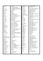
No Terminal Name I/O
Description
P.OFF
P.Failure
Reset/
Release
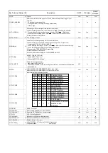
64 VBI1/CHARA
O
Terminal for both NAVI Writing and OSD REC Writing.
1. During NAVI writing (During recording in JET NAVIGATOR is ON)
At NAVI data "H" being written : High is output
At NAVI data "L" being written : Low is output
At except NAVI data being written : Low is output
2. During OSD REC (During recording in OSD REC is ON)
During OSD letters (Except the masking) being written : High is output
Except OSD letters being written : Low
* Other than above condition : Hi-z
Low / Hi-Z
Low / Hi-Z
Low / Hi-Z
65 UNLOADING(H)
O Control terminal for the Unloading operation.
Low
Low
Low
66 FLD_CS
O
Chip select signal for FIP driver.
*Active: "Low" *Non-active: "High"
(Normal ope.)
Low
Low
67 LOADING(H)
O Control terminal for the loading operation.
Low
Low
Low
68 IC.DATA.OUT
O Timer-Bus signal for peripheral ICs control: Data output
(Normal ope.)
In
Hi-Z
69 IC.DATA.IN
I
Timer-Bus signal for peripheral ICs control: Data input
(Normal ope.)
In
In
70 IC.DATA.CLK
O Timer-Bus signal for peripheral ICs control:Clock outout
(Normal ope.)
In
Hi-Z
71 IIC.CLK
O Serial communication terminal (IIC) for IC3001/FM audio IC.
(Normal ope.)
In
Hi-Z
72 IIC.DATA
I/O Serial communication terminal (IIC) for IC3001/FM audio IC.
(Normal ope.)
In
Hi-Z
73 125Hz/ROM.CORE
O
ROM Correction confirmation mode:
* ROM correction setting bit is "ON": "High".
* ROM correction setting bit is "OFF": "Low" is existed.
(Other than ROM Correction confirmation mode, this terminal is the output
terminal of internal clock for main clock adjustment.:Outputting the 125Hz.)
(Normal ope.)
Low
Low
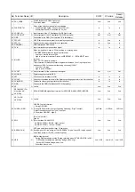
74 CAP R/F
O
The rotation direction control terminal of the capstan driver.
*RVS="High" *FWD="Low".
Low
Low
Low
75 NC
O Low fix.
Low
Low
Low
76 CAP.ET
O
Power supply terminal for the capstan motor control.
(Conpared with the driver reference voltage, when it is "low", current will be cut. Also
when it is "high", the rotation speed will be accelerated.)
High
PWM=0V
Low
High
PWM=0V
77 CYL.ET
O
Power supply terminal of the cylinder motor control:
(Conpared with the driver reference voltage, when it is "high", current will be cut.
Also when it is "low", the rotation speed will be accelerated. (Max:2.8V))
Low
PWM=2.800
V
Low
Low
PWM=2.800
V
78 P.FAIL(L)
I
Input terminal for the power failar detection.
Power failar : "Low".
In
In
In
79 S.REEL.PULSE
I
Input terminal of the S.Reel pulse.
In
In
In
80 T.REEL.PULSE
I
Input terminal of the T.Reel pulse.
In
In
In
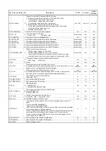
81 SP(L)
O
REC MODE DATA
*N2H/P3H:"Low"
*N4H/N6H/N10H/P6H/P9H:"High"
Low
Low
Low
82 EX.FF/REW (L)
I/O
Control signal filter select terminal in FF/REW mode.
*During FF/REW: Hi-Z
*Except FF/REW: Low
Low
Low
Low
83 P.ON(H)
O
ON/OFF control terminal for the VCR Power.
*Power ON : "High" *Power OFF : "Low"
Low
Low
Low
84 AVR (L)
I/O Simplified AI playback ON/OFF control.
Low
Low
Low
85 SQPB (H)
I
The distinction results whether S-VHS or VHS of the playback tape is input in VV
mode.
*"Low" is input: VHS tape playback.
*"High" is input: S-VHS tape playback.
NOTE: When the MESECAM (H) terminal receives "High", above result is invalidated
and the tape is judged to VHS tape playback.
*In case of model having SQPB function, ON/OFF setting of SQPB is performed with
above result, Envelope voltage and result wheather the CTL pulse exists not.
*In case of model not having SQPB function, above result is disregarded, and the
VCR is always set to SQPB = off.
In
In
In
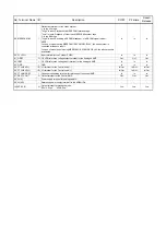
86 FG.AMP.OUT
O Output terminal for the Capstan FG AMP signal.
Out
Out
Out
87 FG.AMP.IN
I
Input terminal for the Capstan FG AMP signal.
In
In
In
88 GND(A)
-
GND for Analogue circuit.
-
-
-
Содержание NV-HV61GN
Страница 20: ...3 1 2 DETAIL OF DISASSEMBLY METHOD 1 REMOVAL OF THE TOP PANEL Remove 2 Screws A Remove 2 Screws B Fig D2 20 ...
Страница 21: ...2 REMOVAL OF THE BACK PANEL Remove 2 Screws C Remove Screw D Unlock 4 Tabs E Fig D3 21 ...
Страница 29: ...10 2 CASING PARTS SECTION 29 ...
Страница 30: ...10 3 PACKING PARTS SECTION 30 ...
Страница 31: ...11 REPLACEMENT PARTS LIST 31 ...
Страница 41: ...C4537 ECJ2VC1H560G CHIP CAPACITOR 41 ...
Страница 44: ...D2002 B0AAED000003 DIODE 44 ...
Страница 47: ...Q1152 2SC3311ASA TRANSISTOR 47 ...
Страница 49: ...R1502 ERJ3GEYJ273V CHIP RESISTOR 49 ...
Страница 54: ...W519 ERJ3GEY0R00V CHIP JUMPER 54 ...
Страница 109: ...4 1 3 PARTS NAME OF R4 MECHANISM Fig M2 ...
Страница 139: ...34 ...


