background image

– 8-7 –

8.3.1.  Getting Started


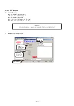
1. To run the program, execute the Service Tool icon on the desktop. The following window will appear:

8.3. Calibration Procedure

3.

Click on "option" to change the COM port. The function is password protected to prevent accidental change to settings.

The password is "Compal_PV1" and is case sensitive. The password must be entered before any changes to the

configuration can be made.

1)

Connection Setup: COM Port

Select the COM port to which the data cable is connected. Default is COM1.

2)

Select Personal INI File

2.

A message log window also appears at the bottom of the main window to display the processing and status information.

After selecting the correct COM port and Personal INI File, click "Apply" to enable the setting.

Содержание EB-X100

Страница 1: ...ncy Range 925 960 MHz 1805 1880 MHz Tx Rx separation 45 MHz 95 MHz RF Channel Bandwidth 200 kHz Number of RF channels 174 374 Speech coding Full rate Half rate Enhanced Full rate Operating temperature 10 C to 55 C Type Class 4 Handheld Class 1 Handheld RF Output Power 2 W maximum 1 W maximum Modulation GMSK BT 0 3 WAP GPRS WAP 2 0 GPRS Class 4 Connection 8 ch TDMA Voice digitizing 13 kbps RPE LTP ...

Страница 2: ...N 1 1 1 1 Purpose of the Manual 1 1 1 2 Structure of the Manual 1 1 1 3 Servicing Responsibilities 1 1 2 GENERAL DESCRIPTION 2 1 2 1 General 2 1 2 2 Features 2 1 2 3 Handportable Main Kits 2 1 3 OPERATING INSTRUCTIONS 3 1 3 1 General 3 1 3 2 Controls and Indicators 3 1 3 3 Liquid Crystal Display 3 2 3 4 Text Entry Edit 3 2 3 5 Menu Structure 3 3 4 TECHNICAL SPECIFICATIONS 4 1 4 1 Tx Characteristic...

Страница 3: ...5 5 18 1 External I O 5 15 5 18 2 LCD Module Interface Signals 5 16 5 18 3 Camera Module Interface 5 17 5 18 4 SIM Interface 5 17 5 18 5 Battery Connector 5 17 5 18 6 Interfaces and Test Points 5 18 6 DISASSEMBY REASSEMBY INSTRUCTIONS 6 1 6 1 General 6 1 6 1 1 ESD Handling Precautions 6 1 6 2 Disassemby 6 2 6 2 1 Lower Case Assembly and Main PCB Removal 6 2 6 2 2 LCD Removal 6 4 6 2 3 Keypad Membr...

Страница 4: ... 1 Case and Cover Parts List 9 1 9 2 Main PCB Assembly 9 3 10 BLOCK DIAGRAMS 10 1 10 1 Baseband 10 1 10 2 RF Band 10 2 11 CIRCUIT DIAGRAMS 11 1 11 1 Main PCB Logic 11 1 11 2 Main PCB RF Band 11 2 11 3 Main PCB IOTA 11 3 11 4 Main PCB COMPANION 11 4 12 LAYOUT DIAGRAMS 12 1 12 1 Main PCB Top View 12 1 12 2 Main PCB Bottom View 12 2 ...

Страница 5: ...elephone system operating on GSM Digital Cellular Networks 1 2 Structure of the Manual 1 3 Servicing Responsibilities The manual is structured to provide service engineering personnel with the following information and procedures 1 General and technical information provides a basic understanding of the equipment kits and options together with detailed information for each of the major component pa...

Страница 6: ...ull Rate Half rate and Enhanced Full Rate EFR speech codec 2 Dual Band E GSM 900 and GSM 1800 operation 3 Tegic T9 Text Entry 4 Voice Ringer 5 Desktop Hand free function comprising integral echo cancellation and noise suppression 6 Wireless Application Protocol WAP Browser 7 Backup Battery 8 Downloadable polyphonic melody ring tones 9 Clock Calculator and Currency Converter 2 3 Handportable Main K...

Страница 7: ...tery requires charging The battery icon flashes during charging Status Pane Icon Displays a small icon related to the current status of the telephone Telephone is roaming on a non home network To use the Call Divert feature or the telephone has Call Diert set Shows there is a Voicemail incoming Shows that vibration alert is switched on Indicates that the phone is in silent mode no tones Flashes to...

Страница 8: ...that the Extended character set has been selected T9 indicates that Tegic T9R predictive text mode is selected Displays a small icon according to the current menu level Name Personal Icon E Mail 2 Icon Location Number Icon on Mobile Phonebook Hotkey Dial Icon Group Icon Ring Alert Type Icon E Mail 1 Icon Tel Number 3 Icon Tel Number 2 Icon Tel Number 1 Icon Name Personal Icon Indicates the current...

Страница 9: ...reases or decreases volume Send Key Makes a call End Key Ends a call or switches the telephone on off when pressed and held Option key Primarily used for accessing the Phonebook or switching character types Cancel Key Used mainly to cancel the current operation and return to the previous menu level In some menus it has other functions Digit keys Enter wild numbers or pauses when pressed and held W...

Страница 10: ...pha Entry 3 4 1 Character Set Key Assignments Alpha entry is used to enter alphanumeric characters in to the Phonebook Short Messages and Greeting Message areas The keypad of Type A Key T9 Normal Greek Extended Numeric Character Operation Alternatives 0 P_ Punctuation i 1 abc A B C a b c Α Β Γ A Ä Å Æ B C Ç a ä å æ à b c 2 def D E F d e f Ε Ζ D E É F d e é è f 3 ghi G H I g h i Η Θ Ι G H I g h i ì...

Страница 11: ... ü ù v 8 wxyz W X Y Z w x y z Χ Ψ Ω W X Y Z w x y z 9 Shift Lock Space Each time a key is pressed it will display the next character When another key is pressed or no key is pressed for a short time the cursor will move to the next position To cycle between Greek characters Α Β Γ extended characters A Ä Å numerals 0 9 and normal characters A B C press Pressing will move the cursor up or down or le...

Страница 12: ...Auto answer Short press Camera Games Contacts Start Browser My Media Alarm Calender Calculator Sound recorder Shortcut key Long press Call service Calls Service changes Connections Show my number Phone Settings Call diverts Voice calls Fax calls Data Calls Cancel all Security Phone lock Call bar PIN PIN2 Fixed dial Network New network Search mode My Phone Sounds Ring tone Preinstalled My Sounds Me...

Страница 13: ...ts All SIM Phone Groups Group 1 Group 2 Contacts list Create SIM Phone Memory status My numbers Voicemail Hot key dial Contacts Messages My Pictures My Animations My Sounds Memory status My Media Bookmarks Newentry Start Browser Settings Browser Wall Breaker Move Box Games Clock Time date Format Games Alarms Sound recorder Auto power on Auto power off Calculator Melody composer Calendar Applicatio...

Страница 14: ...dulation Offset from Centre Frequency kHz Maximum Level Relative to Carrier dB Offset from Centre Frequency kHz Maximum Level dBm 100 0 5 200 30 250 33 400 60 600 to 1800 60 4 1 4 Output RF Spectrum due to Switching Transients E GSM 900 GSM 1800 400 19 22 600 21 24 1200 21 24 1800 24 27 Measurement conditions for output RF spectrum measurements Frequency Span 0 Hz Measurement Bandwidth 30 kHz Vide...

Страница 15: ...100 kHz 300 kHz 36 36 500 MHz to 1 GHz 0 to 1 MHz 100 kHz 300 kHz 36 36 1 GHz to 12 75 GHz 0 to 10 MHz 100 kHz 300 kHz 30 30 1 0 1 710 GHz Excl relevant TX band 10 MHz 300 kHz 1 MHz 30 E GSM 880 MHz to 915 MHz 30 MHz 3 MHz 3 MHz 30 36 1 710 1 785 GHz DCS 1710 MHz to 1785 MHz off from edge of and the Rx bands relevant Tx band 30 1 785 12 75 GHz 925 MHz 960 MHz 1805 MHz 1880 MHz Relevant TX band 1 8...

Страница 16: ...onditions HT Static Conditions Minimum No of samples Minimum No of samples Minimum No of samples Minimum No of samples Test Limit error rate Test Limit error rate Test Limit error rate Test Limit error rate TCH FS FER 4 478 α 13 400 0 122 α 164 000 class Ib RBER 0 32 α 1 500 000 0 41 α 20 000 000 class II RBER 8 333 600 000 7 5 24 000 9 333 30 000 2 439 8 200 Channels Propagation conditions TU hig...

Страница 17: ...SM 900 GSM 1800 FR 600 kHz to FR 800 kHz FR 800 kHz to FR 1 6 MHz FR 1 6 MHz to FR 3 MHz 915 MHz to FR 3 MHz FR 3 MHz to FR 980 MHz FR 600 KHz to FR 800 KHz 1785 MHz to FR 3 MHz 835 MHz to 915 MHz 980 MHz to 1000 MHz 100 KHz to 835 MHz 1000 MHz to 12 75 GHz 100 KHz to 1705 MHz 1705 MHz to 1785 MHz 1920 MHz to 1980 MHz 1980 MHz to 12 75 GHz 70 70 80 90 90 113 113 90 90 _ _ _ _ 70 70 80 87 87 113 10...

Страница 18: ...0 MHz 1930 MHz 1990 MHz RX Bandwidth 35 MHz 75 MHz 25 MHz 60 MHz TX Bandwidth 35 MHz 75 MHz 25 MHz 60 MHz Duplex Spacing 45 MHz 95 MHz Number of Channels 174 374 124 299 AFRCN Channel Numbers 0 124 512 885 128 251 512 810 975 1023 1st TX Channel 880 2 MHz 1710 2 MHz 824 8 MHz 1850 2 MHz Ch 975 Ch 512 Ch 128 Ch 512 Last TX Channel 914 8 MHz 1784 8 MHz 848 8 MHz 1909 8 MHz Ch 124 Ch 885 Ch 251 Ch 81...

Страница 19: ...Diagram 5 1 2 RF Function Block Serial Interafce GSM900 GSM1800 2 4 N divider Phase Comp Phase Comp 3 6GHz R div M div LNA900 LNA1800 VC1 VC2 F321 F322 PA ENA LNA900IN LNA1800IN U321 TR SW ENB ENB ENB ENB U301 PA ENB ENB I Q I Q PAD APC ...

Страница 20: ... 1710 MHz 1785 MHz 90 3 MHz 104 8 MHz 1354 7 MHz 1414 5 MHz GSM 850 824 MHz 849 MHz 82 42 MHz 105 55 MHz 1359 93 MHz 1424 922 MHz GSM 1900 1850 MHz 1910 MHz 97 37 MHz 112 34 MHz 1460 68 MHz 1516 606 MHz RX RX LO E GSM 900 925 MHz 960 MHz 925 2 MHz 959 8 MHz GSM 1800 1805 MHz 1880 MHz 1805 2 MHz 1879 8 MHz GSM 850 869 MHz 894 MHz 869 2 MHz 839 8 MHz GSM 1900 1930 MHz 1990 MHz 1930 2 MHz 1989 8 MHz ...

Страница 21: ... 8 V DCS TX 2 4 V 2 8 V 0 0 V 0 2 V GSM DCS RX 0 0 V 0 2 V 0 0 V 0 2 V Rxqn Rxqp Rxip Rxin Txqn Txqp Txip Txin U341 U321 U301 F322 F321 U342 Transceiver LNA LE APC AFC VC1 VC2 Data CLK PA module Tx VCO LO Quad band TR switch Quad band PA 26 MHz Fref TxDCS PCS TxGSM TxDCS PCS TxGSM ANT GSM RF SAW DCS PCS RF SAW ...

Страница 22: ...and Block Diagram The EB X100 Baseband is built around a U2 GSM baseband LSI One chip Calypso_G2 carries out signal processing with DSP and CPU and the U3 IOTA provides the analogue interface The highly integrated nature of the chips means that each can contain a large number of functions RF I F SIM interface Voice band interface Baseband interface RF digital control lines I and Q lines AFC Power ...

Страница 23: ...oring of GSM baseband processing Working from an event table referring to a GSM TDMA time base the TPU activates tasks to control DSP peripherals with respect to the time constraints related to GSM sequencing one quarter of bit time accuracy The types of events that are controlled in this way are Open TX window Close RX Window etc Figure 5 5 Keypad Circuit Diagram TSPACT 1 M14 PAENA RF TSPACT 2 L1...

Страница 24: ...d which can display up to 17 characters x 6 rows plus two rows of icons It can accommodate Chinese and large character sets Features 8 Colour Silicon TFT 1 4 inch display module for mobile phones or handy electrical equipments 8 Transmission type 8 TN mode 8 Line inversion mode 8 18bit CPU interface 8 Constructions 8 Display format Colour TFT Transmission type 8 Display mode Normally White 8 Displ...

Страница 25: ...ck is built into G2_Lite The module is synchronic by a 32 768 kHz crystal and has a backup power source provided by a button capacitor G2_Lite has a clock auto compensation function to take into account any inaccuracies of the crystal This is able to calibrate out crystal tolerance drift by writing to the compensation registers This calibration can provide adjustments 555 6ppm in 0 0085 ppm increm...

Страница 26: ...d from a 2 85 V supply a low impedance dynamic speaker must be used The GSM Standard requires that the receiver audio frequency response must fit within the mask shown below The phone is designed to meet requirements with a Type 1 artificial ear Figure 5 8 Handheld GSM Transmit Audio Frequency Response Mask Figure 5 9 Handheld GSM Receive Audio Frequency Response Volume Level PGA Volume Total Gain...

Страница 27: ... scaler and 16 bits register define the timer clock duration The watchdog timer receives a 928 kHz clock signal from the G2_LITE clock module A combination of pre scaler and timer register gives a time range of 1 078 µs to 9 039 s The general purpose timers receive a 812 5 kHz clock signal Timer range is between 2 4615 µs and 20 649 s Timer 1 Function Buzzer Timer Setting Tone frequency Timer 2 Fu...

Страница 28: ...de Ni MH cells Figure 5 10 Power Management Block Diagram VBAT UPR VCRAM VRSIM VRRAM VRMEM VSDBB VRDBB VRABB VCMEM VLMEM VCDBB VCIO2 VBAT BACKUP VCABB VCIO1 Sel 2 8 V Sel 1 8 V BACKUP ABB VRPC Core RRTC 1 3 V 1 5 V 1 8 V 10 µA RABB 2 8 V 50 mA ABB Analogue Core RSIM 1 8 V 2 9 V 10 mA RRAM 1 8 V 2 8 V 50 mA RMEM 1 8 V 2 8 V 60 mA RDBB 1 3 V 1 5 V 1 8 V 120 mA RIO 2 8 V 100 mA ABB Digital Core I O B...

Страница 29: ... in G2_Lite starts running software using 32 kHz clock and also starts 13 MHz clock The following Power Down sequence can only be started by G2_Lite setting the DEVICE_OFF bit in IOTA or in emergency case when VBAT 2 7 V or VBAT Vbackup VBAT 2 8 V 1 If emergency case INT1 is set low by IOTA 2 IOTA starts an internal 150 µs watchdog timer to allow G2_Lite to shutdown 3 ONNOFF signal is reset to dea...

Страница 30: ... module The CMOS sensor includes 8 Image Sensor Array 352 x 288 resolution 8 Timing Generator 8 Analog Processing Block 8 A C Converters 8 Output Formatter 8 Digital Video Port 8 SCCB Interface The phone will be power down two minutes after generating a Low battery Alarm The CPU within the phone controls Battery charging If external power is detected and the temperature is within specified limits ...

Страница 31: ... Module Dimension 8 x 8 x 6 12mm Approximation Weight 0 7g Approximation Resolution 300 TV Line Center 250 TV Line Corner GA 8228A lens Optical A D Brightness Gamma Image Array 352 x 288 Gain WB Hue Saturation MUX R G Analogue Processing Output Formatter Column Sense Amps Row Select Control Registers To all circuits B Y Cb Cr Data Formatting Digital Video Port Windowing VREF Y 7 0 1µF RESET PWDN C...

Страница 32: ...eceive data 5 CTS Clear to send 6 RXD Receive data 7 TXD Transmit data 8 RTS Request to send 9 DSR Data set ready 10 TMS TMS 11 ACC_PWR Power Supply 12 VACCID Analogue Input 13 TDO Data out 14 GND Power supply and digital signal ground N B B N N N B B N B N N B 2 85 V 2 85 V 2 85 V 2 85 V 2 85 V 2 85 V Case Front External I O Connector Power Connector 1 14 ...

Страница 33: ...PCA552A G1 15 D9 Data bus No Connect 16 D10 Data bus SPCA552A G2 17 D11 Data bus SPCA552A H1 18 D12 Data bus SPCA552A J1 19 D13 Data bus SPCA552A H2 20 D14 Data bus SPCA552A J2 21 D15 Data bus SPCA552A G3 22 D16 Data bus SPCA552A H3 23 D17 Data bus SPCA552A J3 24 RESET System Reset SPCA552A G6 25 RS Select Register at H Index status Control at L SPCA552A D2 26 GND LED Power Supply Ground for LED 6...

Страница 34: ...YUV Video Component Output bit 0 SPCA552A C6 12 Y1 YUV Video Component Output bit 1 SPCA552A B6 13 Y2 YUV Video Component Output bit 2 SPCA552A A6 14 Y3 YUV Video Component Output bit 3 SPCA552A A5 15 GND System Ground DGND 16 Y4 YUV Video Component Output bit 4 SPCA552A B5 17 Y5 YUV Video Component Output bit 5 SPCA552A C5 18 Y6 YUV Video Component Output bit 6 SPCA552A A4 19 Y7 YUV Video Compone...

Страница 35: ...ITCHONOFF TP9 CLK13M_OUT TP10 PWON TP11 VRTC TP12 VCHG TP13 RTS TP14 CTS TP15 MMI_INT TP16 RX TP17 TX TP18 DSR TP19 TDI TP20 TDO TP21 TCK TP22 TMS TP23 VBAT TP24 BATTEMP TP25 RnW TP26 nCS2 TP27 MSCI_FSY TP28 MSCI_CLK TP29 MSCI_TXD TP30 MSCI_RXD TP31 TPU WAIT TP32 BYPASS TP33 GPIO2 Main PCB SUB PCB TP34 SP TP35 SP TP36 EARP TP37 EARN ...

Страница 36: ...common ground point Wrist Strap A QUICK RELEASE SKIN CONTACT DEVICE WITH A FLEXIBLE CORD WHICH HAS AN INTEGRAL SAFETY RESISTOR OF BETWEEN 5 2 kΩ AND 1 2 MΩ SHALL BE USED Containers All containers and storage must be of the conductive type WARNING The equipment described in this manual contains polarized capacitors utilizing liquid electrolyte These devices are entirely safe provided that neither a...

Страница 37: ...the back of the handset 2 Use the T5 screwdriver to remove the five case screws located inside the lower case 3 Carefully prize apart the Upper Case Lower Case creating a gap at the base I O connector Insert the Case Separation Tool into the gap created and gently slide the tool until the hooks are separated 6 2 Disassembly ...

Страница 38: ... 6 3 4 Separate by gently twisting the Upper Case Lower Case 5 Lift the PCB Board from the Lower Case 6 Push the hook and lift the internal Antenna Box from the PCB Board ...

Страница 39: ... Main PCB Using tweezers open the cover of the FPC connector before removing the LCD Module from the PCB 8 Remove the Camera Module and Shielding Cover from the PCB Board using tweezers 9 Remove the Shielding Cover from PCB Board using tweezers ...

Страница 40: ...5 10 Remove the Frame of the Shielding Case as picture shown below 11 Remove Speaker and speaker cushion from internal Antenna Box 12 Remove the Vibrator Receiver and Keypad from Upper Case using tweezers ...

Страница 41: ... 6 6 13 Using tweezers remove the Microphone from the Lower Case 1 Locate the Microphone into the Lower Case 2 Fit the Vibrator Receiver and Keypad into the Upper Case 6 3 Reassembly ...

Страница 42: ...7 3 Put the Speaker Cushion Speaker into Antenna Box press the Speaker from left to right side 4 Reassemble Shielding Cover into PCB Board 5 Reassemble the Camera Module and Shielding Cover into PCB Board ...

Страница 43: ...y into the PCB Board 7 Use the tweezers to open the FPC connector then insert the LCD flexi strip Close the FPC connector and hook the side of PCB Board Assemble the LCD module to the PCB Board 8 Locate the PCB Board inside the Lower Case ...

Страница 44: ... 6 9 9 Re attach the Upper Case to the Lower Case 10 Fit the five screws inside the Lower Case as shown and tighten with the T5 screwdriver 11 Put in the Battery Pack and close the Battery Cover ...

Страница 45: ...ocedures are described in Section 8 CAUTION The Printed Circuit Board PCB used in this telephone has been manufactured using Lead Free solder SPARKLE ECO SOLDER Part No ESC F3 M705 0 3 Lead Free solder has a higher melting point than Lead solder typically 30 40 C higher Always use a high temperature soldering iron When using a soldering iron with temperature control it should be set to 370 10 C 70...

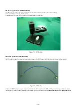
Страница 46: ...ween the PCB Assembly and external test equipment It is required for RF calibration Figure 7 1 Dummy Battery A cable with SMA female connector is provided to make the RF connection An SMA to N Type male adaptor will be required to connect the Repair Jig to the service equipment Cable losses for the RF connection are 0 5 dBm GSM 900 and 0 7 dBm GSM 1800 A replacement RF Probe for the Repair Jig is ...

Страница 47: ...item Figure 7 5 RF Cable Figure 7 4 RF Cable A cable with SMA female connector is provided to make the RF connection An SMA to N Type male adaptor will be required to connect the Jig to the service equipment Cable losses for the RF connection are 0 5 dBM GSM 900 and 0 7 dBM GSM 1800 RF Cable Part No 73PV104001W The RF cable provides the necessary connections between the PCB Repair Jig RF Adapter a...

Страница 48: ...acts as a base station providing all the necessary GSM signalling requirements and also provides GSM signal measuring facilities Figure 7 6 Data Cable Figure 7 7 Power Cable Power Cable Part No 3WZ001130AAA The power cable provides the necessary connections between the PCBA repair jig dummy battery and external power supply ...

Страница 49: ...computer with RS232 interface and running Microsoft Windows 95 98 XP or 2000 7 GSM test station 8 EB X100 Service software The EB X100 Service software should be installed onto the main drive of the personal computer The RF cable is connected to the GSM test station via suitable adaptor The 3 8 V supply is connected to the RF Adaptor and PCB Repair Jig with power cable NOTE A suitable test SIM car...

Страница 50: ...ery to ensure steady voltage to phone Dmtool_v8 x xx 1 Overview Service Tool is an application that integrates the following functions 1 Data Reserve function Some data fields like Phone books Calibration data etc can be stored into files with this function If data is lost use use this function to restore the original data back to the handset 2 Re Flash function Use to download the new versions of...

Страница 51: ...n be selected The default setting is RS232 Turbo DL 3 Select the All Mode Check Box B Dmtool will update the BootCode Region flash block 0 when the user download the MainCode to the handset Default setting is the Skip Mode this will not update the BootCode Region ...

Страница 52: ... to the download list Click the Remove Icon B To remove one select download mot file from the download list Click the Clear Icon B To clear all download mot file from the download list Clicking the Add button will open a Browse window which is used to select the download file ...

Страница 53: ...ocess Click the Abort Icon B Abort the download process Click the Close Icon B Abort the download process and close the application 7 Add mot file to the tool and press Execute button After that press the power key in handset the Interface shows as below ...

Страница 54: ...s complete the target sector information data will be compared with the binary data in the PC RAM buffer If the data in these two buffers is identical the status window will change green and the message PASS will be displayed below it This indicates the download was successful with no errors occurring ...

Страница 55: ... 8 6 10 If any errors were found i e there were differences in data between the two buffers the Dmtool will report in which block of code the error was found ...

Страница 56: ... The password is Compal_PV1 and is case sensitive The password must be entered before any changes to the configuration can be made 1 Connection Setup COM Port Select the COM port to which the data cable is connected Default is COM1 2 Select Personal INI File 2 A message log window also appears at the bottom of the main window to display the processing and status information After selecting the cor...

Страница 57: ...re to enter the proper parameters for your RF calibration and test environment and click Apply Select Test Platform and Address Check box for ADC calibration Check box if DC Source available Input Cable Loss for RF Connection ...

Страница 58: ...ly enter Factory Test Mode and start to read data Wait for Reading Data finish shown on the log list The status of the process can be viewed on the progress bar NOTE Before performing any Service Tool function except reflash reflexing switch on the handset first If a SIM card is inserted wait until the Network searching is complete and then start the Service Tool function If the Network search tak...

Страница 59: ... seen on the progress bar 3 Restart the handset to ensure that user data has been written back 8 4 2 Mobile Kit 1 In Download frame the options Flex Only Language Pack Only or Main Code Only can be selected 2 Click to select the desired version of flex file language pack file or main code Note that the selected flex language pack and main code should all have the same version number Unmatched vers...

Страница 60: ...alibration of gain value AFC Calibration of frequency error and slope APC Calibration of power for each level PC 1 Snapshot of Calibration Screen CAUTION Before calibration you must check parameter of instrument Is it correct Calibration System list Select Mobile Type and Band Choose Cali bration type Exit Calibration ...

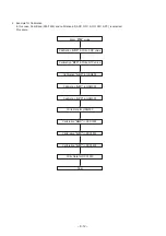
Страница 61: ... selected Procedure Enter FTM mode Calibration ADC Write ADC value Calibration NTC Write NTC value Calibration AGC in GSM900 Calibration AFC in GSM900 Calibration APC in GSM900 Write Data for GSM900 Calibration AGC in DCS1800 Calibration AFC in DCS1800 Calibration APC in DCS1800 Write Data for DCS1800 Final ...

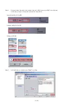
Страница 62: ...ctly to the PC Switch on the handset and click on FTM It will automatically enter Factory Test Mode and start to read data for calibration Step 2 Press Next to continue Step 3 Click ADC Step 3 1 Select 4 2 V and click OK Step 3 2 Select 3 4 V and click OK ...

Страница 63: ...bration temperature of battery in NTC High 40 C Step 4 Press Next to continue Step 5 Click on NTC for battery temperature calibration The purpose of NTC is to prevent the battery temperature becoming too high or too low NTC High 40 C approve of range in 233 to 170 6 9 5KΩ 4 83 KΩ NTC Low 0 C approve of range in 965 to 671 33 9 KΩ 21 6 KΩ ...

Страница 64: ... calibration NTC Low NTC is complete Click on AGC Step 6 Press Next to continue Step 7 Before proceeding with Gain and RSSI check configure the GSM Test Set as follows If a CMU200 is used refer to Annex notex2 1 for Configuration If an HP8960 is used refer to Annex notes2 2 for Configuration ...

Страница 65: ... RSSI value press OK to next channel In this case channel 1 channel 49 channel 85 channel 975 Step 9 AGC calibration is complete press Next to continue Generator setting for Cmu200 Analyser setting for Cmu200 Setting for HP8960 Change channel To chan 1 935 2 MHz ...

Страница 66: ...lick AFC to start AFC calibration If a CMU200 is used refer to Annex notex2 1 for Configuration If an HP8960 is used refer to Annex notes2 2 for Configuration Step 11 AFC calibration is complete press Next to continue ...

Страница 67: ...efer to Annex notes2 2 for Configuration Step 13 Click each button in turn for each power level Referring to the table on the right of the screen adjust the GSM Test Set Analyzer Generator to the required value When the parameter is set press Next to continue Operation Level 5 and Level 6 to examples Note Level 5 parameter value must be decreased Level 6 parameter value must be increased ...

Страница 68: ... 8 19 ...

Страница 69: ... 8 20 ...

Страница 70: ... 8 21 Step 14 Write data GSM900 to the handset and press Next to continue Step 15 After configure parameter of instrument click AGC find gain value and RSSI of full channel ...

Страница 71: ...channel In this case channel 512 channel 596 channel 788 channel 836 channel 872 Step 17 AGC calibration is complete press Next to continue Change channel To chan 512 1805 2 MHz Step 18 Write data DCS1800 to the handset and press End to finish in this procedure ...

Страница 72: ... 85 dBm 2 RF level used 85 dBm Unused 20 dBm Unused 20 dBm Unused 20 dBm CMU200 3 RF Channel 3 RF Channel 3 RF Channel 4 Transmission 4 Transmission 4 Transmission Burst Continuous Continuous 5 Cable lose 5 Cable lose 5 Cable lose 6 Bit modulation Off Annex notes2 1 AGC AFC Please Configure as follows CMU200 8 Change to GSM900 Analyser Generator Non Signalling mode 8 Change RF level Used TS 85 dBm...

Страница 73: ... 8 24 8 Change channel to ch62 in Analyser GSM850 ch190 GSM1800 ch699 GSM1900 ch662 as below 8 Change cable lose of AF RF as below ...

Страница 74: ...nge to GSM900 Analyser Generator Non Signaling mode 8 Change RF level Used TS 85dBm and RF level Unused TS 20dBm in Generator Switch on Generator 8 Change channel to ch62 in Generator GSM850 ch190 GSM1800 ch699 GSM1900 ch662 8 Change Transmission mode to Burst 8 Change Bit modulation to OFF in Generator as below ...

Страница 75: ... 8 26 8 Change channel to ch62 in Analyser GSM850 ch190 GSM1800 ch699 GSM1900 ch662 as below 8 Change cable lose of AF RF as below Annex notes3 2 APC Configure as follows HP8960 ...

Страница 76: ... 8 27 Modify Cable lose 8 4 4 RF Auto Instrument and Address Choose Mobile Type and Band Mobile Phone Info Doing Calibration only Exit RF Test Doing Call Test only Doing Calibration Call Test ...

Страница 77: ... 8 28 8 To download calibration data and measurement data from handset Click button A Calib Call Calibration Measurement ...

Страница 78: ...andset Click button C Call Test When making a Call Test it is necessary for the handset to have a test SIM card inserted which takes extra time to search for the network and hence takes longer to enter Factory Test Mode FTM This calibration process saves time since a test SIM card is not required ...

Страница 79: ...et the password to the factory default 0000 8 Press Power Cycle to exit the Factory Test Mode and restart the handset Before reading and updating handset specific data check that the handset is connected to the PC Switch on the handset Error Message Description 1 FTMx FTMxx FTMxxx Can t Open FTM 2 Open FTM Fail Time Out Open FTM Fail Time Out 3 Ka_init Bad Ka_init Wrong Calibration initial fail 4 ...

Страница 80: ... METALLIC BLACK 2511G66004W UPPER CASE ASSY LIGHT BLUE 302 3104G66001W DIAL KEY ENGLISH 3104G66021W DIAL KEY BOPOMOFO 3104G66031W DIAL KEY STROKE 3104G66061W DIAL KEY RUSIAN 3104G66071W DIAL KEY ARABIC 303 3109G66001W MET DOME 304 3052G66004W SHIELD CASE 305 3052G66003W SHIELD CASE 306 3052G66005W CAMERA SHIELD CASE REF NO PART NO DESCRIPTION 307 23A1G66001W ANTENNA ASSY 308 2512G66001W LOWER CASE...

Страница 81: ...C CAPACITOR 100nF 10V C61 1310452211W CERAMIC CAPACITOR 100nF 10V C62 1310452211W CERAMIC CAPACITOR 100nF 10V C64 1310452211W CERAMIC CAPACITOR 100nF 10V C65 1310452211W CERAMIC CAPACITOR 100nF 10V C66 0710414111W FIXED RESISTOR 100K 1 16W C69 1322046111W CERAMIC CAPACITOR 22pF 50V C70 1322046111W CERAMIC CAPACITOR 22pF 50V C71 1322046111W CERAMIC CAPACITOR 22pF 50V C72 1322046111W CERAMIC CAPACIT...

Страница 82: ...W CERAMIC CAPACITOR 4 7uF 6 3V C342 1310146111W CERAMIC CAPACITOR 100pF 50V C343 1322046111W CERAMIC CAPACITOR 22pF 50V C344 1310146111W CERAMIC CAPACITOR 100pF 50V C345 131R516111W CERAMIC CAPACITOR 1 5pF 50V C346 1310146111W CERAMIC CAPACITOR 100pF 50V C347 1310551211W CERAMIC CAPACITOR 1uF 6 3V C348 1310452211W CERAMIC CAPACITOR 100nF 10V C349 1310551211W CERAMIC CAPACITOR 1uF 6 3V C350 1310452...

Страница 83: ... R37 0722214111W FIXED RESISTOR 2 2KΩ 1 16W R38 0722414111W FIXED RESISTOR 220KΩ 1 16W R40 0715014111W FIXED RESISTOR 15Ω 1 16W R41 07R0014111W FIXED RESISTOR 0Ω 1 16W R42 0710114111W FIXED RESISTOR 100Ω 1 16W R50 1010010411W BLOCK RESISTOR 10Ω R51 0720118121W FIXED RESISTOR 20Ω 1 10W R52 0733014111W FIXED RESISTOR 33Ω 1 16W R53 0710314111W FIXED RESISTOR 10KΩ 1 16W R54 0722414111W FIXED RESISTOR ...

Страница 84: ...LATOR 26MHz VR1 2011001532W VARISTOR 5 5V 33pF VR2 2011001532W VARISTOR 5 5V 33pF VR3 2011001532W VARISTOR 5 5V 33pF VR4 2011001532W VARISTOR 5 5V 33pF VR5 2012002931W VARISTOR 9V 33pF VR6 2012002931W VARISTOR 9V 33pF VR7 2011001532W VARISTOR 5 5V 33pF VR8 2012002931W VARISTOR 9V 33pF VR9 2011001532W VARISTOR 5 5V 33pF VR10 2012002931W VARISTOR 9V 33pF VR11 2011001532W VARISTOR 5 5V 33pF VR12 2011...

Страница 85: ... I and Q lines AFC Power ramp signal J6 Speaker Melody control lines Key pad interface UART J1 Camera Module CON1 SIM CONN J3 Earphone Jack LS1 Receiver MIC1 Microphone U3 IOTA U2 Calypso G2_Lite LCD Module U10 Flash S RAM U8 Backend IC Keypad RTC 32 kHz J4 Battery J5 IO_Connector U17 Melody IC M1 Vibrator BT1 RTC Battery T ...

Страница 86: ... 10 2 10 2 RF Band Serial Interafce GSM900 GSM1800 2 4 N divider Phase Comp Phase Comp 3 6GHz R div M div LNA900 LNA1800 VC1 VC2 F321 F322 PA ENA U321 ENB ENB ENB ENB U301 ENB ENB I Q I Q PAD ...

Страница 87: ...DQ R4 100K RXIR_IRDA X_A1 BDR VDR VCLKRX BFSX BFSR BDX BCLKX IO6 K10 N13 N12 P12 L11 M11 N11 SVDD_EN MCSI_CLK IO11 N10 VDDS MIF B6 VDDS MIF A4 VDD A5 VDD B12 C22 100n C15 100n VDD M1 VDD N14 VDDPLL F11 C2 100n MCUEN 2 IO13 KBC4 XDIO2 IO0 TPU WAIT SDI SDA SCLK INT1n nSCS1 X_A 2 nSCS0 SCL SDO INT10n L8 M5 N3 M9 P9 N9 L9 K8 KBR0 XDIO3 KBR1 XDIO4 KBR2 XDIO5 KBR3 XDIO6 KBR4 XDIO7 LT PWL KBC0 NFIQ KBC1 ...

Страница 88: ...1 100n DCS_PA GSM_PA DGND DGND VRF RF_LE DCS_TX GSM_TX TEMP_SEN U342 Crystal_26MHz IN 1 GND 2 OUT 3 GND 4 31 14 15 16 18 19 21 22 23 24 31 37 38 39 40 41 48 49 4 2 1 3 C371 47p C372 12p C373 7p VR341 HVC375B C374 33n C341 2 2U C370 1n LBTXOUT1 HBTXOUT1 LBTXOUT2 HBTXOUT2 L342 15nH L342 15nH C357 7p C355 12p R345 0 R350 1K R348 1K 4 2 1 3 DGND DGND DGND DGND DGND DGND VBAT2 44 VBAT1 46 LNAPCSP SIOUT...

Страница 89: ...IN4 C38 100p C149 100n C416 33p C48 33n C218 100n R208 2 2K VR30 5 5V 33p C152 1U C407 33p C411 33p C150 100n DGND DGND DGND DGND DGND DGND R82 39 R83 39 R84 20K C138 5 5V 33p C137 5 5V 33p C138 100n C140 5 5V 33p C141 5 5V 33p CON1 CLK 1 I O 2 RST 3 VPP 4 VCC 5 GND 6 TOP VIEW SIO5 SRST5 SCLK5 R22 10K DGND VLMEM L8 VRABB A9 R16 100K R17 NM 100K R24 100K VRIO2 M2 VRDBB VSDBB M11 VRIO1 M1 VRRAM M7 V...

Страница 90: ... C51 1U R30 0 C53 100n C54 100n G7 J9 H9 H8 HBUS3 HBUS0 HBUS1 HBUS2 H4 DGND DGND DGND DGND VBAT LCMLED_EN LCMLED_EN LCM BACK LIGHT FB 1 GND 2 EN 3 VOUT 4 VBAT 5 C118 1U C153 1U C40 22p L3 C240 22p R40 15 D10 1 2 D2 D0 D1 D8 D9 D10 D11 D14 D15 D12 D13 D6 D4 D5 D7 D3 DGND DGND DGND DGND D 7 D 6 D 5 D 4 D 3 D 2 D 1 D 0 D 1 2 D 9 D 1 3 D 8 D 1 5 D 1 4 D 1 0 D 1 1 VRMEM DGND DGND LED LCM_RESET LED LCM_...

Страница 91: ...219 C133 C134 C131 C130 C135 VR30 C406 R71 R29 VR7 VR24 C74 C73 C72 C90 C91 C70 C71 D12 D14 D11 D9 D7 D8 R44 R43 R46 C88 C89 R47 R41 R45 C69 VR5 VR6 VR1 VR3 VR2 C239 R98 R97 R91 C430 C429 C428 C427 C426 C425 C424 C423 C422 C421 C420 C234 C238 C237 C236 C235 C224C233 C225C232 C226C231 C219C230 C220C229 C221C228 C222C227 C116 C405 S20 S8 S18 S2 S21 S19 S17 S1 S16 S11 S6 S5 S4 S3 S10 S7 S9 S15 S14 S1...

Страница 92: ...355 C354 C60 C18 C19 R12 R33 C53 C414 L323 C310 C327 C328 R321 L302 C311 L301 U342 L321 L322 VR4 R67 R54 R55 R35 R37 R36 R42 R64 C99 TP29 TP27 TP25 TP26 TP23 TP20 TP6 TP1 R27 L3 D10 D2 TP5 TP11 TP15 TP16 TP8 TP14 TP7 TP2 TP24 TP22 TP21 C54 R8 R2 C1 R3 R5 R4 R6 C5 C9 C10 C16 R90 C110 C115 C367 C364 C153 C240 C42 C44 C46 C43 R28 C15 C103 C95 C94 R59 R76 R15 R19 C31 C38 C351 R346 R345 R344 R343 C350 ...

Отзывы: