background image

One Stop Systems, Inc.                                                                                                          OSS-wanPCI-CxT1E1 User Manual  

Rev. A    


                                 4 

Communications Controller  

Conexant CN8474A communications controller


The OSS-wanPCI-CxT1E1 uses a Conexant CN8474A communications controller as the HDLC processing engine.  


• 

The CN8474A Multichannel Synchronous Communications Controller (MUSYCC) is an advanced, multichannel, 

synchronous communications controller that formats and deformats 128 HDLC channels in a single CMOS IC.  

• 

The MUSYCC provides HDLC channels for internetworking applications such as Frame Relay, X.25, Signaling System 7 

(SS7), ISDN D-channel signaling, and LAN/WAN data transport.  

• 

Under minimal host supervision, the MUSYCC manages a linked list of channel data buffers in host memory by performing 

direct memory access (DMA) for the 128 channels, Tx and Rx.  


The MUSYCC interfaces with four independent serial data streams, such as T1/E1/J1 signals, and then transfers data across the 

peripheral component interface (PCI) bus to system memory at a rate of 132 MBps. The OSS-wanPCI-CxT1E1 will operate for both 

T1 (1.544MHz) or E1 (2.048MHz). Logical channels can be mapped as any combination of DS0 time slots to support ISDN 

hyperchannels (Nx64Kbps) or as any number of bits in a DS0 for subchanneling applications (Nx8Kbps)  


COMET framer


The four PMC Sierra Framer interface components (PM4351 COMETs) allow the software to select between T1 (100 Ohm), E1 

(120 Ohm), and J1 configurations.  

I/O  

T1/E1/J1 ports


The OSS-wanPCI-CxT1E1 supports four T1/E1/J1 ports. Four onboard COMET chips provide the framer and LIU supporting the 

four T1/E1/J1 ports. The CSU components reside on the module. The tip and ring for each port are routed to fully shielded RJ48C 

connectors mounted behind the PMC bezel. 

T1/E1/J1 and COMET register settings 

COMET register settings impact the TI/E1/J1 pulse waveform and therefore, your telecom (FCC part 68 and CEMark) approval. 

Register tables are available in the PM4351 COMET COMBINED T1/E1 TRANSCEIVER/FRAMER DATASHEET from PMC-Sierra 

(PMC-970624). See Chapter 6, In-System Programmable Logic Device (iSPLD), for information on the initialization of the waveform 

registers and equalizer registers. 


Front Panel 

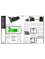
The front panel will have 1, 2 or 4 RJ48 ports. The front panel for the OSS-wanPCI-C4T1E1 is shown below. 


Содержание Multi Port E1

Страница 1: ...One Stop Systems Inc OSS wanPCI CxT1E1 User Manual Rev A Multi Port T1 E1 J1 PCI Adapter OSS wanPCI CxT1E1...

Страница 2: ...upport is available for T1 E1 or J1 The OSS wanPCI CxT1E1 can use both SS7 or HDLC protocols Initial Set Up Unpacking Instructions 1 If the carton is damaged when you receive it request that the carri...

Страница 3: ...on between the RJ 48 jack on the adapter and the RJ 48 jack in your wall or test system 5 Turn on power to the computer Adapter installation is complete 6 Reverse the above procedure to remove the boa...

Страница 4: ...or both T1 1 544MHz or E1 2 048MHz Logical channels can be mapped as any combination of DS0 time slots to support ISDN hyperchannels Nx64Kbps or as any number of bits in a DS0 for subchanneling applic...

Страница 5: ...CI CxT1E1 supports four T1 E1 J1 ports Four PM4351 COMET chip sets provide the framer and LIU to support the four T1 E1 J1 ports The CSU components reside on the OSS wanPCI CxT1E1 The tip and ring for...

Страница 6: ...AD 30 AD 31 3 3V AD 29 21 22 AD 28 GND AD 26 AD 27 23 24 GND AD 25 AD 24 3 3V 25 26 IDSEL C BE 3 3 3V AD 23 27 28 AD 22 GND AD 20 AD 21 29 30 GND AD 19 AD 18 3 3V 31 32 AD 16 AD 17 3 3V C BE 2 33 34...

Страница 7: ...rd serial numbers are stored in a Microchip 93LC46A and packaged in a small outline integrated circuit This device can hold 1024 bits organized in a 128x8 format The PCI host reads and writes to this...

Страница 8: ...to be at zero 9 Periodically read the data in bit until a one is found 10 Write a byte with both the chip select and data out bits at zero 11 Disable EEPROM Reading from the EEPROM 1 Set the chip sele...

Страница 9: ...One Stop Systems Inc OSS wanPCI CxT1E1 User Manual Rev A 9 Clock Frame Pulse Routing Matrix continued...

Страница 10: ...up the access time and enables the EBus for individual accesses 4 Depending on how you want the board configured write to the MCLK register next to configure which ports are E1 and which are T1 Then...

Страница 11: ...t specific mode of operation Serial EEPROM A 500ns delay is necessary for both read and write cycles of the serial EEPROM Since the MUSYCC s data cycle time is approximately 300ns the algorithm by whi...

Страница 12: ...ck Select Register Any or all of the COMETs can provide the clock for data synchronization The host via the MCSR decides which COMET provides the clock At reset each COMET provides the clock for its p...

Страница 13: ...ort 1 1 COMET 1 MCLK E1 Port2 0 COMET 2 MCLK T1 Port2 1 COMET 2 MCLK E1 Port3 0 COMET 3 MCLK T1 Port 3 1 COMET 3 MCLK E1 Type 1 0 00 4 Ports Available 01 1 Ports Available 10 2 Ports Available Other v...

Страница 14: ...YCC transfers this interrupt from the EBus to the PCI INTB pin when enabled in the Global Configuration Descriptor The PCI host processor reads the interrupt register to determine which device was res...

Страница 15: ...in The board JTAG chain is not supported at the PCI connection The following is the JTAG chain order For 2 port and 1 port options on board 0 ohm resistors are used to bypass the appropriate COMETs No...

Отзывы: