


JTAG/OCE10 Test Access Port (TAP)
MSC711x Application Development System (MSC711xADS) Reference Manual, Rev. 1
Freescale Semiconductor
43
You can connect the JTAG device to the MSC711xADS in one of two ways:
• Direct to the appropriate external JTAG/OCE10 device.
• Host-to-personal computer parallel port connection.
5.5.1
Direct Connection to External JTAG/OCE10 Device
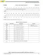
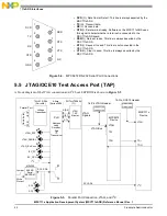
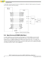
The JTAG header on the MSC711xADS provides a connection between the MSC711xADS board and any external
compatible JTAG converter. Figure 5-6 shows the connector (located at P14) and its pins. The pins are described in
Table 5-2.
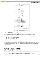
Figure 5-6. JTAG/OCE10 Port Connector
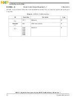
Table 5-2. JTAG/OCE10 Pins
Pin
Signal
Attribute
Description
1
TDI
I
Transmit Data In
The JTAG serial data input of the ADS, sampled on the rising edge of TCK.
2
GND
P
Digital GND
Main GND plane.
3
TDO
O
Transmit Data Output
This the MSC8101’s JTAG serial data output driven by Falling edge of TCK.
4
GND
P
Digital GND
Main GND plane.
5
TCK
I
Test Port Clock
Shifts data in/out and to/from the MSC7116EVM JTAG logic. Data is driven on the falling
edge of TCK and is sampled both internally and externally on its rising edge. TCK is pulled
up internally by the MSC7116.
6
GND
P
Digital GND
Main GND plane.
7
N.C
—
Not connected.
8
KEY
—
No pin (serves for correct plug insertion).
1
3
5
7
9
11
13
2
4
6
8
10
12
14
TDI
TDO
TCK
N.C.
RESET
3.3V
N.C.
GND
GND
GND
KEY (No Pin)
TMS
NC
TRST