

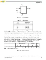


Power Supply
MSC711x Application Development System (MSC711xADS) Reference Manual, Rev. 1
Freescale Semiconductor
27
3.3 Power Supply
The MSC711xADS uses the following voltages:
• 5 V: (Command converter).
• 3.3 V: (MSC711x and MPC8272 I/O and for most of the components)
• 2.5 V: (SSTL components: the DDR chip and the DDR interface in the MSC711xADS).
• V
REF
: (1.25 V for DDR active termination).
• 1.5 V: MPC8272 core voltage.
• 1.2 V: MSC711x core voltage.
These voltages are derived from the 12 V main power supply (switch P23).
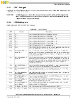
The MSC711xADS maximum currents demands are:
• 100 mA for the I/O at 3.3 V.
• 240 mA for the SDDR at 2.5 V.
• 511 mA for the core at 1.2 V.
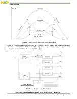
The MSC711xADS has three distinct power supplies (1.2 V core, 2.5 V DDR I/O, and 3.3V standard I/O). When
the board is powered up or powered down, the following sequences of operations must be followed.
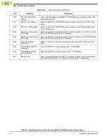
The power-up sequence is as follows:
1.
Turn on the highest supply (3.3 V standard I/O).
2.
Turn on the 2.5 V DDR I/O supply.
3.
Turn on the lowest supply (1.2 V core).
The power-down sequence is as follows:
1.
Turn off lowest supply (1.2 V core).
2.
Turn off 2.5 V DDR IO.
3.
Turn off highest supply last, 3.3 V standard I/O.
CAUTION:
Latch up forward biasing of ESD devices and excessive currents can lead to severe
device damage. To avoid this problem, a proper power-up and power-down
sequence at the board level must performed.