


Memory Map
MSC711x Application Development System (MSC711xADS) Reference Manual, Rev. 1
Freescale Semiconductor
29
Memory Map/Programming Model
4
This chapter presents a recommended memory map and describes the MSC711xADS registers in detail. The
MPC8272 memory controller is used as a chip-select generator to access on-board (and external) memories, saving
board area and reducing cost and power consumption while increasing flexibility. When a
CS
region assigned to a
buffered memory is disabled via the BCSR, the local data transceivers are disabled during access to that region to
prevent possible contention on data lines. Table 3-1 shows the MPC8272 chip-select assignments to the various
memories/registers on the MSC711xADS.
4.1 Memory Map
All accesses to the MPC8272 memory slaves are controlled by the MPC8272 memory controller. Therefore, the
memory map is reprogrammable. After a hard reset, the debugger checks for the size, delay, and type of the Flash
memory on the board and programs the memory controller accordingly. The SDRAM and the Flash memory
respond to all types of memory access; that is, problem /supervisory, program/data, and DMA. The memory map
shown in Table 3-2 is a recommended memory map. However, the devices addresses can be moved around the
map, according to your needs.
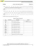
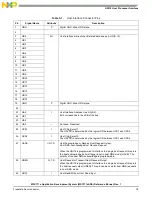
Table 3-1. MPC8272 Chip-select Assignments
Chip Select
Assignment
Bus
CS0
Flash memory
60x (buffered)
CS1
BCSR
60x (buffered)
CS2
SDRAM
60x (main)
CS3
PMC E1/T1 framer (via the BCSR)
60x (buffered)
CS4
PEF20451 TSI switch (via the BCSR)
60x (buffered)
CS5
SLIC-SLAC MPI (via the BCSR)
60x (buffered)
CS6
HDI CS0
60x (buffered)
CS7
HDI CS1
60x (buffered)
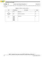
Table 3-2. Memory Map
Address Range
Memory Type
Port Size
Memory Size
0x00000000–0x03FFFFFF
60x SDRAM
64 bit
64 MB
0x04000000–0x044FFFFF
Empty Space
5 MB