


MSC711x Application Development System (MSC711xADS) Reference Manual, Rev. 1
24
Freescale Semiconductor
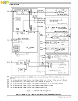
Board-Level Functions
• OCE10/JTAG port. Asserting the
HRESET
line connected to the OCE10/JTAG port connector directly generates
a hard reset for only the MSC711x processor.
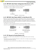
• Manual hard reset. Both the MPC8272 and the MSC711x processors have their own
HRESET
push button. In
addition, you can generate a manual hard reset for the MSC711x by toggling a bit in BCSR3.
• Internal sources. Both the MSC711x and MPC8272 have internal sources that can generate an
HRESET
in
response to specific events.
A hard reset causes the MPC8272 and MSC711x processors to reset all their internal hardware except for PLL
logic and reacquires the hard-reset configuration from its current source (for the MPC8272). Since hard reset also
resets the refresh logic for dynamic RAMs, their content is lost as well. The MPC8272
HRESET
can generate an
HRESET
to the MSC711x processor, depending on the JP6 position. The MSC711x
HRESET
affects only the
MSC711x and does not generate an MPC8272
HRESET
.
CAUTION:
Contention on the HRESET may cause permanent damage to either board logic
and/or to the MPC8272 and the MSC711x processors. To prevent contention,
always drive HRESET with an open-drain gate.
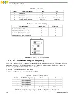
When a hard reset is applied to the MPC8272 (externally as well as internally), it samples the Hard Reset
Configuration Word (HRCW). This configuration word can be taken from the Flash memory or BCSR (the most
significant 8 bits of the data bus), depending on the JP5 position.
3.2 Clocking
There are three main clock circuits on the MSC711xADS board:
• MPC8272 system clock
• PCI clock
• MSC711x system clock
3.2.1
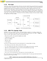
MPC8272 System Clock
The MPC8272 requires a single clock source as the main clock source. All MPC8272 60x bus timings are
referenced to the main clock input,
CLKIN1
. The timing ratio between the main clock input and the bus clock is 1:1,
with internal skew elimination via a PLL. A 100 MHz 3.3 V clock oscillator is connected to a low inter-skew buffer
(U10) to split the load between all clock consumers on both boards. To provide a clean clock input for proper
operation, special care is taken to isolate and terminate the clock route between the on-board PLL and the
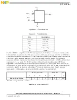
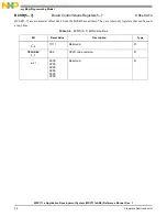
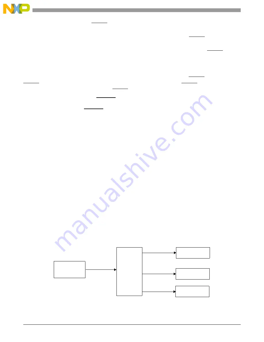
MPC8272. The main clock scheme is shown in Figure 3-1
.
Figure 3-1. Main Clock Generator Scheme
CLK GEN
100 MHz
60x SDRAM
Expansion
Mictor
Low
Skew
Buffers