


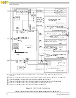


Board Control and Status Registers (BCSRx)
MSC711x Application Development System (MSC711xADS) Reference Manual, Rev. 1
Freescale Semiconductor
33
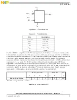
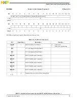
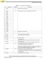
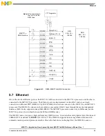
BCSR2 is a read-only status register. It can be read at any time.
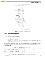
BCSR2
Board Control Status Register 2
Offset 0x8
Bit
0
1
2
3
4
5
6
7
8
9
10
11
12
13
14
15
H8B
DBREQ BM0
BM1
SWTE HDSPOL HDDS PQDMA
—
TYPE
R
R/W
R
RESET
0
1
1
0
Bit
16
17
18
19
20
21
22
23
24
25
26
27
28
29
30
31
—
TYPE
R
RESET
0
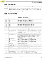
Table 4-3. BCRS2 Bit Descriptions
Bit
Reset Value
Description
Setting
H8B
0
0
MSC711xADS HDI 8-Bit mode.
0
16-bit HDI mode.
1
8-bit HDI mode.
DBREQ
1
0
MSC711xADS debug mode request.
0 Normal
run
mode.
1 Debug
mode.
BM0
2
0
MSC711xADS boot mode 0–1.
00 HDI.
01
I
2
C.
BM1
3
0
SWTE
4
0
MSC711xADS software watchdog.
0
Watchdog disable.
1 Watchdog
enable.
HDSPOL
5
0
MSC711xADS HDI strobe polarity.
0 Active
low.
1 Active
high.
HDDS
6
1
MSC711xADS HDI double data strobe.
0
Single strobe.
1 Double
strobe.
PQDMA
7
1
MPC8272 DMA DREQ3 signal value according to
PQDMA.
• PQDMA = 0
→
DREQ3 =
HRRQ.
• PQDMA = 1
→
DREQ3 = HRRQ
and CS6.
—
8–31
0
Reserved. Write to zero for future compatibility.