NXP Semiconductors KITFS85SKTEVM Скачать руководство пользователя страница 6

NXP Semiconductors

UM11183

KITFS85SKTEVM evaluation board

UM11183

All information provided in this document is subject to legal disclaimers.

© NXP B.V. 2019. All rights reserved.

User guide

Rev. 2.0 — 20 February 2019

6 / 50

Table 1. Compensation network

Components

VPRE 450 kHz

VPRE 2.2 MHz

C18/C19

6.8 nF

1.5 nF

C14/C15

150 pF

22 pF

R6/R10

3.57 kΩ

16.9 kΩ

LPRE

4.7 µH or 

6.8 µH

1.5 µH

, 2.2 µH or 4.7 µH

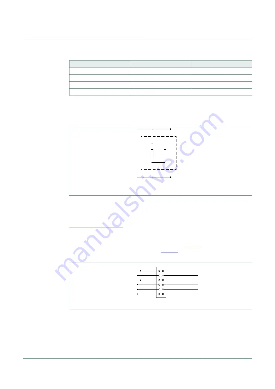
4.1.4 BUCK1 and BUCK2 multiphase configuration

The board is designed to work independently with BUCK1 and BUCK2. Due to R11 and

R145, it is possible to connect both connectors together and work in multiphase.

aaa-032767

BUCK1

BUCK2

R11

0

DNP

R145

0

DNP

Figure 4. BUCK1 and BUCK2 multiphase configuration

4.1.5 SPI/I2C

The SPI and I2C buses are connected to KL25Z MCU. The user can use either one or

the other. The choice can be done at start of the FlexGUI or at any time after launch (see

Section 8 "Using FlexGUI"

).

This kit uses a KL25Z MCU to communicate with FlexGUI. However, if the user wants

to connect the SPI to another MCU, this is possible. In this case, remove J28 and

appropriate jumpers to disconnect the KL25Z MCU (see 

Figure 5

) and connect the

external MCU on J30 connector as shown in 

Figure 6

. In addition to this change, make

sure that the VDDIO voltage domain is the same on MCU side and SBC side.

aaa-032768

2
4
6
8
10
12

RSTb_SH
FS0b_SH
MISO_SH
MOSI_SH

[3] RSTb
[3] FS0b
[3] MISO
[3] MOSI

[3] CSB

[3] SCLK

SCLK_SH
CSB_SH

1

J28

3
5
7
9

11

Figure 5. SPI connection to KL25Z

Содержание KITFS85SKTEVM

Страница 1: ...technical support services Should this evaluation kit not meet the specifications indicated in the kit it may be returned within 30 days from the date of delivery and will be replaced by a new kit NXP...

Страница 2: ...a good flexibility This board supports FS84 FS85 family of devices 2 Finding kit resources and information on the NXP web site NXP Semiconductors provides online resources for this evaluation board a...

Страница 3: ...e FlexGUI software allows access to the registers in read and write mode All regulators are accessible through connectors Nonuser signals like DC DC switcher node are mapped on test points Digital sig...

Страница 4: ...gnal or regulator status Support OTP fuse capabilities USB connection for register access OTP emulation and programming Voltage monitoring jumper setting Note Due to the socket all current capabilitie...

Страница 5: ...k R180 27 4 k BUCK3_MON3 BUCK3 VMON_08V J24 1 2 3 GND HDR 1X3 R189 22 1 k R178 68 1 k LDO_MON4 LDO1 VMON_08V J21 1 2 3 GND HDR 1X3 R192 22 1 k R182 68 1 k LDO2 GND R208 22 1 k R207 115 k Figure 2 VMO...

Страница 6: ...R145 0 DNP Figure 4 BUCK1 and BUCK2 multiphase configuration 4 1 5 SPI I2C The SPI and I2C buses are connected to KL25Z MCU The user can use either one or the other The choice can be done at start of...

Страница 7: ...ovided to feed VDDI2C This LDO can also be used to feed VDDIO which is the default implementation The I2C is compatible with 1 8 V or 3 3 V while VDDIO is compatible with 3 3 V and 5 0 V For this reas...

Страница 8: ...hree times using mirror registers The user can first load the mirror register content with the desired contents then decide either to use the device in Emulation mode or to burn the next sector The fi...

Страница 9: ...VSUP_UVH WAKE12VIH SPI I2C OTP pgm OFF PWR UP ON SPI I2C Figure 10 Debug mode entry Figure 11 shows the hardware kit implementation aaa 032762 SW1 SW2 VSUP1 2 FS8500 Debug ref OTP level DBG 8 V 2 1 3...

Страница 10: ...ng voltage switch 12 VBOOST and BUCK3 power supply 13 DEBUG voltage source 14 Compensation network selection 15 VDDIO selection 16 SPI RSTb FS0b connection to MCU 17 RSTb INTb and FS0b signals 18 VMON...

Страница 11: ...m FS84 fit for ASIL B and FS85 fit for ASIL D pin to pin and software compatible The FS85 FS84 is an automotive functionally safe multi output power supply integrated circuit with focus on Radar Visio...

Страница 12: ...frequency tuning 2x linear voltage regulators for MCU IOs and ADC supply external physical layer Configurable output voltage and current capability up to 400 mA DC Standby OFF mode with very low sleep...

Страница 13: ...G 8 0 V Blue DBG pin voltage 8 0 V OTP programming D13 RSTb Red RSTb asserted logic level 0 D14 INTb Red INTb asserted logic level 0 D15 FS0b Red FS0b asserted logic level 0 D16 P3V3_KL25 Green P3V3_K...

Страница 14: ...Table 7 LDO1 LDO2 connector J2 Schematic label Signal name Description J2 1 LDO1 LDO1 power supply output J2 2 LDO2 LDO2 power supply output J2 3 GND Ground Table 8 VPRE connector J3 Schematic label...

Страница 15: ...nit 2 J29 20 GND Ground 4 3 3 4 Program connector J30 Table 10 Program connector J30 Schematic label Signal name Description J30 1 WAKE1 WAKE1 input J30 2 MOSI SPI master output slave input J30 3 VDDI...

Страница 16: ...e Description TP1 GND Ground TP2 GND Ground TP3 LDO2 LDO2 regulator output TP4 LDO1 LDO1 regulator output TP5 VPRE VPRE DC DC regulator output TP6 GND Ground TP7 VBOOST VBOOST DC DC output TP8 BOOST_L...

Страница 17: ...P shunt 3 4 For current measurement insert amperemeter 1 2 BUCK_INQ tied to VPRE J8 BUCK3 input 2 3 BUCK_INQ tied to VBOOST 1 2 LDO1_IN connected to VPRE J9 LDO1 input 2 3 LDO1_IN connected to VBOOST...

Страница 18: ...V J24 VMON3 2 3 VMON3 tied to BUCK3 J25 RSTb 1 2 Reset LED Enabled when jumper is plugged J26 INTb 1 2 Interrupt LED Enabled when jumper is plugged J27 FS0b 1 2 FS0b LED Enabled when jumper is plugged...

Страница 19: ...the Windows PC workstation consists of three steps 1 Install the appropriate Java SE Runtime Environment JRE 2 Install Windows 7 FlexGUI driver 3 Install FlexGUI software package 5 1 Installing the J...

Страница 20: ...evaluation board UM11183 All information provided in this document is subject to legal disclaimers NXP B V 2019 All rights reserved User guide Rev 2 0 20 February 2019 20 50 4 In the SECON FLEX GUI SL...

Страница 21: ...n board UM11183 All information provided in this document is subject to legal disclaimers NXP B V 2019 All rights reserved User guide Rev 2 0 20 February 2019 21 50 5 in the Update Software Driver win...

Страница 22: ...ed in this document is subject to legal disclaimers NXP B V 2019 All rights reserved User guide Rev 2 0 20 February 2019 22 50 6 Select Let me pick from a list of device drivers on my computer and the...

Страница 23: ...oard UM11183 All information provided in this document is subject to legal disclaimers NXP B V 2019 All rights reserved User guide Rev 2 0 20 February 2019 23 50 9 Click Browse 10 In the Locate File w...

Страница 24: ...ormation provided in this document is subject to legal disclaimers NXP B V 2019 All rights reserved User guide Rev 2 0 20 February 2019 24 50 11 In the Install from Disk window click OK 12 If prompted...

Страница 25: ...d in this document is subject to legal disclaimers NXP B V 2019 All rights reserved User guide Rev 2 0 20 February 2019 25 50 13 Close the window when the installation is complete 14 In the Virtual Co...

Страница 26: ...TEVM evaluation board UM11183 All information provided in this document is subject to legal disclaimers NXP B V 2019 All rights reserved User guide Rev 2 0 20 February 2019 26 50 The Virtual Com Port...

Страница 27: ...nstalling FlexGUI software package The FlexGUI software installation requires only extracting the zip file in a desired location 1 If necessary install the Java JRE and Windows 7 FlexGUI driver 2 Down...

Страница 28: ...er Configuration J17 connect 1 2 connect 5 0 V on DBG pin from the USB 2 Configure switches for the configuration Table 17 Switch configuration Switch Configuration SW1 middle position VBAT off SW2 op...

Страница 29: ...he DBG pin level Normal mode is set by tying DBG to ground Debug mode is set by setting DBG voltage to 5 0 V In OTP emulation you can overwrite the mirror registers from a given OTP fuse configuration...

Страница 30: ...0 50 Figure 20 OTP_conf_failsafe_reg spreadsheet example 3 See the OTP_conf_summary sheet to review the complete configuration main and fail safe Figure 21 OTP_conf_summary example 4 Generate the scri...

Страница 31: ...ile in Debug mode all regulators are turned Off 4 Load the mirror registers to work in OTP emulation mode See Section 8 3 Working with the Script editor 5 Unplug jumper J17 1 2 to start the device wit...

Страница 32: ...T of FS_WD_WINDOW 3 FS_I_SAFE_INPUTS 0x51C6 FCCU_CFG 1 0 0x0 0x1 Monitoring by pair FCCU12_FLT_POL 0 1 FCCU1 or 2 0 is a fault 4 FS_I_NOT_SAFE_INPUTS 0xAC18 NOT of FS_I_SAFE_INPUTS 5 FS_WD_ANSWER 0x5A...

Страница 33: ...the FlexGUI application After FlexGUI is launched with the flexgui app bat file the FlexGUI launcher displays available kits Communication bus SPI or I2C can be selected at this level It is also poss...

Страница 34: ...t This change is managed by the onboard MCU to communicate with the desired bus It is also possible to change the clock frequency using this panel Note that in the case of I2C most of the time the def...

Страница 35: ...on that Poll button is enabled 8 3 Working with the Script editor The register and OTP emulation can be configured with the script editor This is particularly useful to try various OTP configurations...

Страница 36: ...6 50 8 3 1 Script text editor Using Script editor you can execute any command either directly or from a file It is also possible to save and modify a script Using the brush symbol it is possible to cl...

Страница 37: ...ers NXP B V 2019 All rights reserved User guide Rev 2 0 20 February 2019 37 50 Figure 27 Build a command The value 0x0800 is sent to the register M_REG_CTRL1 BUCK2DIS The user can then send it to the...

Страница 38: ..._I_NOT_SAFE_INPUTS AC18 SET_REG FS85 safety FS_WD_ANSWER 0x5AB2 SET_REG FS85 safety FS_STATES 0x4000 SET_REG FS85 safety FS_WD_ANSWER 0x5AB2 SET_REG FS85 safety FS_WD_ANSWER 0x5AB2 SET_REG FS85 safety...

Страница 39: ...igure 31 Register map Register map allows access to functional register safety register and write init register which are accessible only during initialization phase Read allows you to read any regist...

Страница 40: ...frequencies and spread spectrum 8 4 3 Regulators The regulator has two main areas Low voltage LV regulators configuration VPRE compensation network calculation Each regulator can either be enabled or...

Страница 41: ...ided in this document is subject to legal disclaimers NXP B V 2019 All rights reserved User guide Rev 2 0 20 February 2019 41 50 Figure 34 Measurements 8 4 5 Interrupt flags This tab allows you to set...

Страница 42: ...sters that can be configured to close the initialization phase Note that the initialization phase is closed by the first good watchdog refresh before 256 ms timeout Figure 36 INIT safety 8 4 7 Diag sa...

Страница 43: ...ary 2019 43 50 Figure 37 Diag safety The FS_Release_FS0b command calculates and sends the right secure16 bit word to release FS0b A simplified way to release FS0b after power up is to first select the...

Страница 44: ...en turns Off Note that the blue LED on the board indicates that an 8 0 V voltage is available on the Debug pin This voltage is used only during the burning process and should not be applied in any oth...

Страница 45: ...n is read from mirror register It is possible to modify it and update the mirror register As an example the slot sequence is filled at start up with the content of OTP fuses Then the user can decide t...

Страница 46: ...laimers NXP B V 2019 All rights reserved User guide Rev 2 0 20 February 2019 46 50 8 4 10 TestMode Mirrors_Main and TestMode Mirrors_Failsafe The TestModeMirrors_Main and TestModeMirrors_FailSafe tabs...

Страница 47: ...documentation downloads and software and tools http www nxp com KITFS85SKTEVM 2 FS8500 product information on FS8500 Safety system basis chip for S32 microcontrollers fit for ASIL D http www nxp com F...

Страница 48: ...s applications or products or the application or use by customer s third party customer s Customer is responsible for doing all necessary testing for the customer s applications and products using NXP...

Страница 49: ...g 5 SPI connection to KL25Z 6 Fig 6 J30 SPI connection 7 Fig 7 VDDIO selection 7 Fig 8 VDDI2C supply 7 Fig 9 OTP configuration 8 Fig 10 Debug mode entry 9 Fig 11 OTP hardware implementation 9 Fig 12 E...

Страница 50: ...Indicators 12 4 3 3 Connectors 13 4 3 3 1 VBAT connector J1 13 4 3 3 2 Output power supply connectors 14 4 3 3 3 Debug connector J29 14 4 3 3 4 Program connector J30 15 4 3 4 Test points 15 4 3 5 Jum...

Отзывы: