


NXP Semiconductors
UM11183
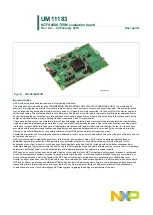
KITFS85SKTEVM evaluation board
UM11183
All information provided in this document is subject to legal disclaimers.
© NXP B.V. 2019. All rights reserved.
User guide
Rev. 2.0 — 20 February 2019
11 / 50
Number
Description
8
Debug connectivity. Access to:
•
VSUP, GND
•
FOUT/FIN
•
PGOOD/RST/FS0b
•
FCCUx
•
Wake2
•
PSYNC, ERRMON, AMUX
•
VMONx
9
Programming
•
SPI bus
•
I2C bus
•
Debug pin
•
VPRE, VSUP, GND
10
Wake1 switch
11
OTP burning voltage switch
12
VBOOST and BUCK3 power supply
13
DEBUG voltage source either from USB (recommended) or from VSUP
14
VPRE compensation network selection, either 2.2 MHz or 450 kHz
15
VDDIO source from device regulators or external sources
16
SPI, RSTb or FS0b can be disconnected between device and MCU
17
RSTb, INTb and FS0b signals available here (device pin level)
18
Allows to select VMON from regulators or a fix 0.8 V
VDDI2C can be selected either 1.8 V or 3.3 V
4.3.1 FS8500/FS8400: Fail-safe system basis chip with multiple SMPS and LDO
4.3.1.1 General description
This device family is part of a global platform FS84 (fit for ASIL B) and FS85 (fit for ASIL
D), pin to pin and software compatible. The FS85/FS84 is an automotive functionally safe
multi-output power supply integrated circuit, with focus on Radar, Vision, ADAS domain
controller, Radio and Infotainment applications. It includes multiple switch mode and
linear voltage regulators. It offers external frequency synchronization input and output, for
optimized system EMC performance.
The FS85/FS84 includes enhanced safety features, with fail-safe output, becoming a full
part of a safety-oriented system partitioning, covering both ASIL B and ASIL D safety
integrity level. It is developed in compliance with ISO 26262 standard. Several device
versions are available, offering choice in number of output rails, output voltage setting,
operating frequency and power up sequencing, to address multiple applications.
4.3.1.2 Features
•
60 V DC maximum input voltage for 12 V and 24 V applications
•
VPRE synchronous buck controller with external MOSFETs. Configurable output
voltage, switching frequency, and current capability up to 10 A peak.
•
Low voltage integrated synchronous BUCK1 converter, dedicated to MCU core supply
with SVS capability. Configurable output voltage and current capability up to 3.6 A
peak.