15
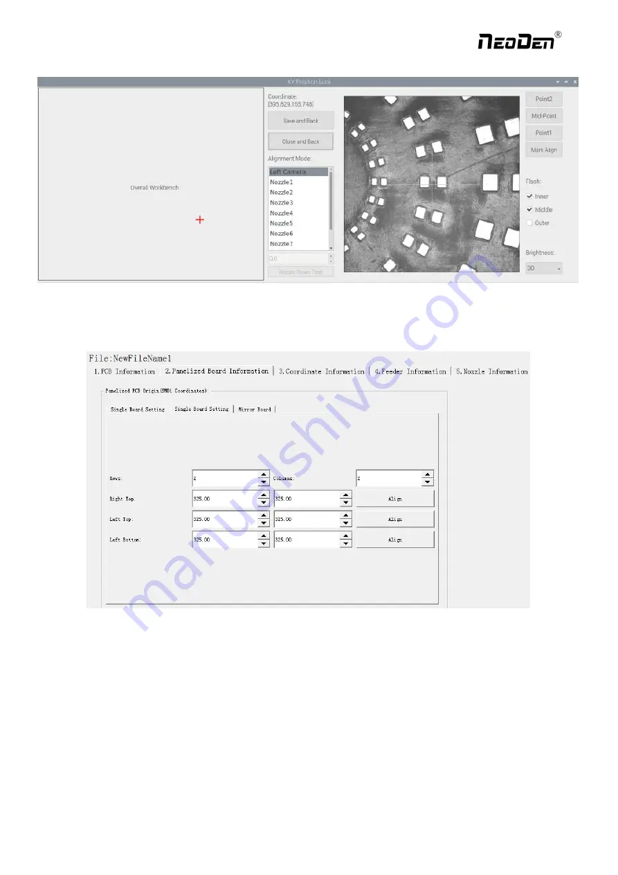
Click “ok”, it will back to the previous interface, click “create panelized list” button, the data which on the panelized list
will change.Can see the “SMD1 information”on the list and do double check via “align”button.
3.1.2
Panelized board
The steps of the panelized board programming are similar with the single board, but need pay some attention to several
points below
The row and column are determined by the positioning of PCB on working area. The direction along the rails is the column,
the direction perpendicular to the rail is row, then please enter data in the row and column.
Please refer to the data collecting method of each position information as following:
●
The data of “left bottom” is collected according to first component in the component list of programming file. Press
“align” of left bottom, find the left bottom panel that is nearest to the left side and nearest to the feeding position, then find
the first component which on the chip list of this panel, align the center of this component. After saving the data, it will
return to the “PCB information” automatically.
Zhejiang
NeoDen Technology Co.,Ltd.
Содержание K1830
Страница 6: ...1 3Working Area Structure Figure 3 Top view of main mounting area 6 Zhejiang NeoDen Technology Co Ltd ...
Страница 7: ...Figure 4 X axis Beam Figure 5 Main Placement Head Camera 7 Zhejiang NeoDen Technology Co Ltd ...
Страница 35: ...8 2 Component Positions Setup 35 Zhejiang NeoDen Technology Co Ltd ...
Страница 44: ...11 Structure and maintenance instruction 11 1 Feeder Brief Introduction 44 Zhejiang NeoDen Technology Co Ltd ...


