Configuration and Installation
Chapter 2
SCXI-1120 User Manual
2-28
© National Instruments Corporation
Timing Requirements and Communication Protocol
Timing Signal
The data acquisition timing signal is SCANCLK.
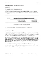
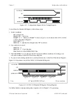
SCANCLK is used to increment MUXCOUNTER on its rising edge. Figure 2-12 shows the
timing requirements of the SCANCLK signal. These requirements will ensure that SCANCLK
is properly transmitted over TRIG0.
T
low
T
high
SCANCLK
T
low
Time low before rising edge
400 nsec minimum
T
high
Time high before falling edge
250 nsec minimum
Figure 2-12. SCANCLK Timing Requirements
For output selection time specifications, refer to Appendix A, Specifications.
Communication Signals
This section describes the methods for communicating on the Serial Peripheral Interface (SPI)
bus and their timing requirements. The communication signals are SERDATIN, DAQD*/A,
SLOT0SEL*, SERDATOUT, and SERCLK. Furthermore, SS* is produced by Slot 0 according
to data acquisition board programming, and SS* timing relationships will also be discussed. For
information on the Slot 0 Slot-Select Register, consult Chapter 4, Register Descriptions.
The data acquisition board determines to which slot it will talk by writing a slot-select number to
Slot 0. In the case of an SCXI-1001 chassis, this write also determines to which chassis the data
acquisition board will talk. Writing a slot-select number is also used in programming the Slot 0
hardscan circuitry. See Chapter 5, Programming, for information on programming the Slot 0
hardscan circuitry.
The following sections detail the procedure for selecting a slot in a particular chassis.
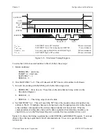
Figure 2-13 illustrates the timing of this procedure with the example case of selecting Slot 11 in
Chassis 9. Notice that the factory-default chassis address for the SCXI-1000 is address 0. For
information on changing the address of your chassis, consult the SCXI-1000/1001 User Manual.
An SCXI-1000 chassis will respond to any chassis number.


