background image

3-1

Chapter 3

Theory of Operation

3.1

Introduction

This chapter provides a detailed theory of operation for the radio components. Schematic diagrams 
for the circuits described in the following paragraphs are located in Figures 5-1 through 5-34.

3.2

Radio Power Distribution

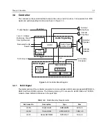
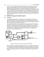
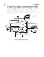
A block diagram of the DC power distribution throughout the radio board is shown in Figure 3-1. Four 
voltage regulators are used as follows:

The 7.5 V battery supplies radio power (UNSWB) directly to the electronic on/off control circuit, audio 
power amplifier, 3.3 V Li-Ion regulator U410, transmitter PA driver and PA Final stage, the Power 
Control IC, and the low battery detect circuit. 

When the radio on/off/volume control is turned on, the switched battery voltage SWB+ from Q400 is 
applied to the various regulators, antenna switch, the 20-pin accessories connector J403, the 40-pin 
keypad/option board connector J400, and the transmit LED. The Vddd source from digital 3.3V 
regulator U400 supplies operating power to the microprocessor, EEPROM, RAM and Flash ROM IC's. 
The Vdda analog 3.3 V regulator (U3201 in 200 MHz models, U203 in 700 MHz models) provides 
operating voltage for the ASFICcmp, VCOBIC, synthesizer IC. The 5 V regulator (U3711 in 200, U202 
in 700)  also powers the synthesizer IC as well as the receiver front end and IF circuitry, the RX and 
TX (700 MHz only) VCO buffers, and the opamp audio gain stage. Some stages are supplied only 
during receive by 5R, switched by Q3721 (200) or Q201 (700 MHz). Regulator voltage routing is 
configurable by jumper placement. All models are configured with R401 and R405 placed, and R402-
4 not placed.

At power up, Q400 is initially turned on by the path through Q403, CR440, and Q405. When C480 has 
charged, this path is disabled, and Q400 is maintained on via a logic high ASFICcmp U404 pin 37, via 
CR440 and Q405.

The radio turns off when either of the two following conditions occur:

Radio on/off/volume control is turned off.

Low battery condition is detected.

If a low battery level or loss of battery voltage is detected by the microprocessor pin 67 through either 
of the above conditions, the radio personality data is stored to EEPROM prior to turning off. At this 
point U404-37 goes low, turning off Q400.

Table 3-1.   Voltage Regulators

Name

200 MHz

700 MHz

Application

3.3 V Reg

U410

U410

Li-lon backup battery charging

Vdda

U3201

U203

Analog 3.3 V source (audio, VCO, synth)

Vddd

U400

U400

Digital 3.3 V source (

µ

P and memory)

5 V Reg

U3711

U202

Analog 5 V source (RF, IF, synth)

Содержание HT1250-LS+

Страница 1: ...ional Radio are trademarks of Motorola Inc LTR is a registered trademark of E F Johnson Company PassPort is a registered trademark of Trident Datacomm Technologies Inc All other product or service names are the property of their respective owners 2002 Motorola Inc All rights reserved Printed in U S A 6864110R12 6864110R12 O ...

Страница 2: ... the SOFTWARE MOTOROLA SHALL NOT BE LIABLE FOR INCIDENTAL OR CONSEQUENTIAL DAMAGES ARISING FROM THE USE OF THIS SOFTWARE With respect to the U S Government if acquired under FAR policy 52 227 19 the SOFTWARE is provided with Restricted Rights and if acquired under DFARS policy 227 7202 then the SOFTWARE is provided only with the commercial rights of this Agreement This license is effective until t...

Страница 3: ...Chart and Specifications 1 3 1 6 Radio Model Information 1 3 Chapter 2 Intrinsically Safe Radio Information 2 1 FMRC Approved Equipment 2 1 2 2 Repair of FMRC Approved Products 2 2 2 2 1 Repair 2 2 2 2 2 Relabeling 2 2 2 2 3 Do Not Substitute Options or Accessories 2 2 Chapter 3 Theory of Operation 3 1 Introduction 3 1 3 2 Radio Power Distribution 3 1 3 3 Keypad PassPort Option Board 3 2 3 4 Contr...

Страница 4: ... 3 11 3 8 3 Harmonic Filter 3 12 3 8 4 Antenna Matching Network 3 12 3 8 5 Power Control Integrated Circuit PCIC 3 12 3 8 6 Temperature Cut Back Circuit 3 12 3 9 700 MHz Receiver 3 12 3 9 1 Receiver Front End 3 13 3 9 2 Receiver Back End 3 13 3 10 700 MHz Frequency Generation System 3 14 3 10 1 Overview 3 14 3 10 2 Fractional N Synthesizer 3 14 3 10 3 Voltage Controlled Oscillator VCO 3 15 3 11 Tr...

Страница 5: ...Oscillator Schematic Diagram 5 12 Figure 5 11 200 MHz Transmitter and Power Control Schematic Diagram 5 13 Figure 5 12 200 MHz Controller Block Diagram 5 14 Figure 5 13 200 MHz Microprocessor Schematic Diagram 5 15 Figure 5 14 200 MHz Memory Schematic Diagram 5 16 Figure 5 15 200 MHz ASFIC Schematic Diagram 5 17 Figure 5 16 200 MHz Audio Power Amplifier Schematic Diagram 5 18 Figure 5 17 200 MHz C...

Страница 6: ...MHz Controls and Indicators Schematic Diagram 5 37 Figure 5 32 700 MHz Keypadd PassPort Board Interface Schematic Diagram 5 38 700 MHz Radio Parts List 5 39 Figure 5 33 PassPort Trunking Controller PCB Board Side 1 2 5 43 Figure 5 34 Keypad PassPort Option Board Schematic Diagram 5 44 ...

Страница 7: ...8 Figure 5 7 200 MHz Receiver Front End Schematic Diagram 5 9 Figure 5 8 200 MHz Receiver I F Schematic Diagram 5 10 Figure 5 9 200 MHz Frequency Synthesizer Schematic Diagram 5 11 Figure 5 10 200 MHz Voltage Controlled Oscillator Schematic Diagram 5 12 Figure 5 11 200 MHz Transmitter and Power Control Schematic Diagram 5 13 Figure 5 12 200 MHz Controller Block Diagram 5 14 Figure 5 13 200 MHz Mic...

Страница 8: ... Schematic Diagram 5 36 Figure 5 31 700 MHz Controls and Indicators Schematic Diagram 5 37 Figure 5 32 700 MHz Keypadd PassPort Board Interface Schematic Diagram 5 38 Figure 5 33 PassPort Trunking Controller PCB Board Side 1 2 5 43 Figure 5 34 Keypad PassPort Option Board Schematic Diagram 5 44 ...

Страница 9: ... 1 Related Documents 1 2 Table 1 2 Radio Model Number Example AAH25MDF4DP5AN 1 3 Table 3 1 Voltage Regulators 3 1 Table 3 2 Radio Memory Requirements 3 3 Table 3 3 MODB VSTBY Supply Modes 3 4 Table 4 1 Recommended Test Tools 4 4 ...

Страница 10: ...viii ...

Страница 11: ...energy awareness information and operating instructions in the Product Safety and RF Exposure booklet enclosed with your radio Motorola Publication part number 68P81095C98 to ensure compliance with RF energy exposure limits Before using this product read the operating instructions for safe usage contained in the Product Safety and RF Exposure booklet enclosed with your radio C a u t i o n ...

Страница 12: ...x Product Safety and RF Exposure Compliance ...

Страница 13: ... 2 Return Instructions In instances where the product is covered under a return for replacement or return for repair warranty a check of the product should be performed prior to shipping the unit back to Motorola This is to ensure that the product has been correctly programmed or has not been subjected to damage outside the terms of the warranty Prior to shipping any radio back to a Motorola warra...

Страница 14: ...o part number is assigned the part is not normally available from Motorola If the part number is appended with an asterisk the part is serviceable by a Motorola depot only If a parts list is not included this generally means that no user serviceable parts are available for that kit or assembly Table 1 1 Related Documents Title Part Number 200 700 MHz Professional Radio Portable Level 1 2 Basic Ser...

Страница 15: ...rmine the RF output power frequency band protocols and physical packages from these numbers The example below shows one portable radio model number and its specific characteristics Table 1 2 Radio Model Number Example AAH25MDF4DP5AN Type of Unit Model Series Freq Band Power Level Physical Packages Channel Spacing Protocol Feature Level Model Revision Model Package AA H 25 M 200 MHz 5 700 MHz C 1 o...

Страница 16: ...1 4 Introduction ...

Страница 17: ...done by the original product manufacturer at one of its FMRC audited manufacturing facilities Unauthorized or incorrect modification of an FMRC Approved Product unit will negate the Approval rating of the product WARNING Do not operate radio communications equipment in a hazardous atmosphere unless it is a type especially qualified e g FMRC Approved for such use An explosion or fire may result WAR...

Страница 18: ...ce FMRC Approval labels shall not be stocked by the repair facility An FMRC Approval label shall be ordered from the original manufacturer as needed to repair a specific unit Replacement labels may be obtained and applied by the repair facility providing satisfactory evidence that the unit being relabeled was originally an FMRC Approved unit Verification may include but is not limited to a unit wi...

Страница 19: ...voltage for the ASFICcmp VCOBIC synthesizer IC The 5 V regulator U3711 in 200 U202 in 700 also powers the synthesizer IC as well as the receiver front end and IF circuitry the RX and TX 700 MHz only VCO buffers and the opamp audio gain stage Some stages are supplied only during receive by 5R switched by Q3721 200 or Q201 700 MHz Regulator voltage routing is configurable by jumper placement All mod...

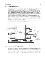
Страница 20: ...amples the voltage levels at the keypad row and keypad column A D inputs and makes a comparison with a map table to identify the key pressed Once the key is identified a corresponding function is executed The LED_EN is set by the codeplug When the value is set to low the LED lights up during power up A high codeplug setting disables this feature Figure 3 2 Keypad PassPort Option Board Block Diagra...

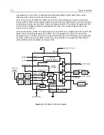
Страница 21: ...re used in all 200 MHz and 700 MHz models unless indicated otherwise in the parts lists Table 3 2 Radio Memory Requirements Reference No Description Type Size U405 Static RAM SRM2B256 32K x 8 U406 Flash ROM AT49HLV010 128K x 8 U407 Serial EEPROM X25128 2 7 16K x 8 External Microphone Internal Microphone External Speaker Internal Speaker SCI to Side Connector Audio Signalling To Synthesizer Mod Out...

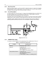
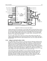
Страница 22: ...he lithium battery back up power when the radio is switched off A MOSFET transistor Q416 switches in the battery supply when Vdd is removed Q416 also provides isolation from BOOT_CTRL function The 3 3V regulator charges the Lithium battery Figure 3 4 RTC Circuit 3 4 4 MODB VSTBY Supply The supply to the MODB VSTBY pin varies depending on the conditions listed in Table 3 3 Table 3 3 MODB VSTBY Supp...

Страница 23: ...r The 200 MHz transmitter consists of the following basic circuits as shown in Figure 3 5 Power amplifier PA Antenna switch harmonic filter Antenna matching network Power control integrated circuit PCIC Figure 3 5 200 MHz Transmitter Block Diagram 3 5 1 Power Amplifier PA The 200 MHz PA consists of two LDMOS devices C65 LDMOS driver IC U3501 MRF1517 LDMOS PA final Q3501 The C65 LDMOS driver U101 p...

Страница 24: ...nic filter output and the 50 ohm SMA style antenna connector J3501 3 5 5 Power Control Integrated Circuit PCIC The transmitter uses the PCIC U3502 to regulate the power output of the radio The current drain of the final device Q3501 is measured as the voltage drop across series resistor R3519 This voltage is then fed back to the automatic level control ALC within the PCIC to regulate the output po...

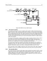
Страница 25: ...eatable passband response The output of the RF amp filter is connected to the passive double balanced mixer consisting of components T3301 T3302 and CR3301 High side injection from the frequency synthesizer is low pass filtered by C3373 6 C3381 and L3327 8 to remove second harmonic energy which may degrade half IF spurious rejection performance and applied to T3302 at a level of 5 dBm The IF outpu...

Страница 26: ...interconnections to the surrounding components Refer to the schematic to identify reference designators The Fractional N synthesizer is powered by regulated 5V and 3 3V provided by U3711 and U3201 respectively 5V is applied to U3701 pins 13 and 30 and 3 3V is applied to pins 5 20 34 and 36 The synthesizer in turn generates a super filtered 4 5V supply VSF from pin 28 to power U3801 In addition to ...

Страница 27: ...V at U3701 pin 47 This voltage is filtered by C3705 6 and C3714 One of the auxiliary outputs of the synthesizer IC pin 48 controls transistor switch Q3721 which outputs a T5 voltage source during transmit and R5 during receive Figure 3 8 200 MHz Synthesizer Block Diagram 3 7 3 Voltage Controlled Oscillator VCO The VCOBIC U3801 shown in Figure 3 9 in conjunction with the Fractional N synthesizer U3...

Страница 28: ...z RF signal from U3801 pin 10 is applied as TX_INJ to the input of the transmitter driver IC U3501 pin 16 via a resistive attenuator pad TX VCO frequency is determined by L3833 C3870 and varactor D3831 Audio from the synthesizer IC is applied as VCO_MOD to varactor D3832 which modulates the transmit VCO Figure 3 9 200 MHz VCO Block Diagram Presc RX TX Matching Network Low Pass Filter Attenuator Pi...

Страница 29: ...with an input signal of 0 3W The PA current drain is typically 1050 mA while operating in the frequency range of 746 794 MHz The PA power output can be changed by varying the C65 LDMOS driver control voltage 3 8 2 Antenna Switch The antenna switch circuit consists of two pin diodes CR101 and CR102 a pi network C106 7 C109 and L103 and three current limiting resistors R101 3 In the transmit mode pi...

Страница 30: ...ge drop proportional to the final device current drain This voltage is then fed back to the automatic level control ALC within the PCIC to regulate the output power of the transmitter The PCIC contains internal digital to analog converters DACs that provide a programmable control loop reference voltage The PCIC internal resistors integrators and external capacitors C142 C144 and C146 control the t...

Страница 31: ...gh IF consists of 2 pole crystal filter FL350 IF amp Q350 2 pole crystal filter FL351 and IF amp Q351 Each crystal filter has a 3 dB bandwidth of 9 0 kHz and a maximum insertion loss of 2 dB The output of Q351 is applied to the input of the receiver IFIC U350 Diode D350 prevents overdriving the IFIC The IFIC is a low voltage monolithic FM IF system incorporating a mixer oscillator two limiting IF ...

Страница 32: ...varying the audio level applied to the synthesizer IC Internally the audio is digitized by the Fractional N and applied to the loop divider to provide the low port modulation The audio is also routed through an internal attenuator for modulation balancing purposes and is available at U201 pin 41 MODOUT This audio signal is attenuated significantly by R211 12 and superimposed on the steering line v...

Страница 33: ... the RF signal from the enabled oscillator is routed from U600 pin 12 through a low pass filter L203 C234 in the synthesizer circuit to the prescaler input of the synthesizer IC U201 pin 32 After frequency comparison in the synthesizer a resultant DC control voltage is used to steer the VCO frequency When the PLL is locked on frequency this voltage can vary between 2 to 9 volts in the RX mode or 3...

Страница 34: ...saver mode In this case both the receive and transmit oscillators as well as the receive transmit and prescaler buffer are turned off Figure 3 14 700 MHz VCO Block Diagram Presc RX TX Matching Network Low Pass Filter Attenuator Pin 8 Pin 14 Pin 10 5V U201 Pin 28 VCC Buffers TX RF Injection U201 Pin 32 AUX4 U201 Pin 3 AUX3 U201 Pin 2 Prescaler Out Pin 12 Pin 19 Pin 20 TX RX BS Switching Network U60...

Страница 35: ...torage features Refer to Figure 3 2 for connector and signal routing from to and through the Radio PTCB and Liquid Crystal Display LCD sub systems 3 11 2 1 Power Supplies The radio supplies regulated Vdd of 3 3 VDC This is used to power the Low Speed Data Filter and Voice Storage circuits The radio also supplies Switched Battery Voltage SWB U612 regulates the SWB to 3 3V which is applied to the PT...

Страница 36: ...cuitry Voice Storage IC U611 provides all the required functionality and is powered from the regulated 3 3 volts from U610 The µP controls U611 via SPI bus lines CLK U611 8 DATA U611 10 and MISO U611 11 To transfer data the µP first selects the U611 via line VS CS and U611 pin 9 Then the µP sends data through line DATA and receives data through line MISO Pin 2 RAC of U611 indicates the end of a me...

Страница 37: ...l alcohol 70 by volume 1 Cleaning External Plastic Surfaces The detergent water solution should be applied sparingly with a stiff non metallic short bristled brush to work all loose dirt away from the radio A soft absorbent lintless cloth or tissue should be used to remove the solution and dry the radio Make sure that no water remains entrapped near the connectors cracks or crevices 2 Cleaning Int...

Страница 38: ...e not accessible some special considerations are required when soldering and unsoldering components The printed through holes may interconnect multiple layers of the printed circuit Therefore care should be exercised to avoid pulling the plated circuit out of the hole When soldering near the 20 pin and 40 pin connectors avoid accidentally getting solder in the connector be careful not to form sold...

Страница 39: ...ch up the first side All solder joints should be smooth and shiny To replace a chip component using hot air Use the hot air hand piece and reflow the solder on the solder pads to smooth it Apply a drop of solder paste flux to each pad Using a pair of tweezers position the new component in place Position the hot air hand piece approximately 1 8 0 3 cm above the component and begin applying heat Onc...

Страница 40: ...ios These tools are also available from Motorola Table 4 1 Recommended Test Tools Motorola Part Number Description Application RSX4043 Torx Driver Tighten and remove chassis screws 6680387A70 T 6 Torx Bit Removable Torx driver bit R1453A Digital readout solder station Digitally controlled soldering iron 0180386A78 Illuminated magnifying glass with lens attachment 0180386A82 6684253C72 6680384A98 1...

Страница 41: ... 5 4 B501 3 2 1 C132 C173 C172 H101 P100 Q111 3 4 R170 R133 R172 CR501 Fuse F501 700 MHz Board 200 MHz Board 24 B501 C431 C433 C434 C436 C437 C453 C535 C3211 C3219 C3220 C3221 C3223 C3224 C3226 C3227 C3228 C3229 C3230 C3231 C3232 C3233 C3234 C3235 C3236 C3238 C3239 C3240 C3241 C3242 C3243 C3244 C3301 C3304 C3305 C3315 C3316 C3317 C3321 C3322 C3323 C3324 C3325 C3326 C3337 C3339 C3701 C3702 C3703 C3...

Страница 42: ...M CS ERROR wrong codeplug checksum reprogram codeplug L400 R421 TP405 VR434 VR450 CR413 Q417 3 4 TP406 J403 20 22 C441 C491 C492 C490 C493 C494 C495 C496 C497 R477 R450 21 1 C471 C472 C473 L401 TP410 VR447 VR449 C443 40 R435 TP401 TP402 C427 C444 C428 RT400 8 5 4 1 U407 J400 C423 E407 E408 E409 R418 R437 R410 SH400 8 21 U405 1 7 22 C426 C425 C429 C424 R408 R492 R429 R478 R428 1 16 U406 17 32 PB503...

Страница 43: ...rrect the problem ESN BAD defective PTCB return to factory for PTCB replacement AppCode Fail defective PTCB firmware reflash PTCB firmware EER Watchdog firmware failure restart radio Unprogrammed programming error use CPS to properly program radio and PTCB ERROR NO PTG no primary talk group use CPS to program zone with a Primary Talk Group Backdoor turn radio off and restart If the error code disp...

Страница 44: ... PTT U409 Pin 53 low Press PTT Q502 2 High Check PB504 Check Q502 2 voltage LED Q502 R501 OK Replace Faulty Component Check Accessories J403 OPT_SEL_1 OPT_SEL_2 Pin 8 9 low Radio could not PTT externally U409 Pin 52 6 low See FGU Troubleshoot ing chart LED should light up Check MCU PTT NO YES YES No No NO YES YES NO YES YES NO NO YES YES NO NO YES NO YES NO YES YES NO NO YES EXT SPKR EXT PTT INT A...

Страница 45: ...o at pin 8 of U3101 Check Controller Yes No Induce or inject 1st IF into XTAL Filter IF Freq 44 85 MHz Audio heard B Yes No Check 2nd Voltage at U3101 Pin 4 Level approx 6 dBm B Yes No Troubleshooting Flow Chart for Receiver Sheet 1 of 2 Check Y3200 If OK check replace U3101 ...

Страница 46: ...1 No Yes Check RF amp Q3302 Stage Check filter between Q3302 T3301 Yes Check T3301 T3302 CR3301 Yes 1st LO O P OK 5 dBm at T3302 Pin 6 Locked Yes Check FGU Yes Trace IF signal from C3200 to Q3200 Check for bad XTAL filter No Yes Q3200 collec tor OK IF signal present Before replac ing U3101 check U3101 voltages trace IF signal path Yes Check for 2 9 VDC Q3200 C Is 5V supply present Check U3711 No N...

Страница 47: ...k PCIC 1 Check Pin Diodes 2 Check Harmonic Filter Inspect Repair Tx Output Network Is Power OK Done Check Drive to Module Is Drive OK Troubleshoot VCO Inspect PA Network Check Power Out of U3501 at Cap C3512 Is Power OK Replace U3501 Is Power OK Replace Q3501 Done Done No Yes Yes No No Yes Low High No Yes Yes No Yes No Troubleshooting Flow Chart for Transmitter ...

Страница 48: ...14 15 of U3701 Replace or resolder necessary components Is RF level at U3701 Pin 32 30 dBm Are C3724 C3723 R3721 R3722 R3723 OK Replace U3701 If R3727 C3726 C3727 are OK then see VCO troubleshooting chart Are Waveforms at Pins 14 15 triangular Do Pins 7 8 9 of U3701 toggle when channel is changed Check programming lines between U409 and U3701 Pins 7 8 9 Replace U3701 Check uP U409 Troubleshooting ...

Страница 49: ...eck U3701 Pin 2 for 3 2V Is U3801 Pin 19 0V in RX Mode AUX 3 Low Change U3801 V ctrl 0V or 13V L3821 L3822 L3823 Open Circuit Change U3801 Change L3821 L3822 L3823 Change U3701 Troubleshoot Q3802 and associated circuitry A A No No Yes Yes Yes No No Yes No Yes No Yes No No Yes Yes Yes No Check R3811 L3811 for dry joint or faulty No Troubleshooting Flow Chart for VCO Yes RF Signal at U3801 Pin 8 No ...

Страница 50: ...PTT U409 Pin 53 low Press PTT Q502 2 High Check PB504 Check Q502 2 voltage LED Q502 R501 OK Replace Faulty Component Check Accessories J403 OPT_SEL_1 OPT_SEL_2 Pin 8 9 low Radio could not PTT externally U409 Pin 52 6 low See FGU Troubleshoot ing chart LED should light up Check MCU PTT NO YES YES No No NO YES YES NO YES YES NO NO YES YES NO NO YES NO YES NO YES YES NO NO YES EXT SPKR EXT PTT INT AU...

Страница 51: ...dio at pin 8 of U350 Check Controller Yes No Induce or inject 1st IF into XTAL Filter IF Freq 73 35 MHz Audio heard B Yes No Check 2nd Voltage at U350 Pin 4 Level Approx 6 dBm B Yes No Troubleshooting Flow Chart for Receiver Sheet 1 of 2 Check Y350 If OK check replace U350 ...

Страница 52: ...o Yes Check RF amp Q301 Stage Check filter FL301 and associated circuitry Yes Check T301 T302 and CR301 Yes 1st LO O P OK 8 dBm at T302 Pin 6 Locked Yes Check FGU Yes Trace IF signal from L304 to Q350 Check for bad XTAL filter No Yes Q350 collec tor OK IF signal present Before replac ing U350 check U350 voltages trace IF signal path Yes Check for 3 0VDC Q350 C Is 5V supply present No No No Yes Yes...

Страница 53: ...ck PCIC 1 Check Pin Diodes 2 Check Harmonic Filter Inspect Repair Tx Output Network Is Power OK Done Check Drive to Module Is Drive OK Troubleshoot VCO Inspect PA Network Check Power Out of U101 at Cap C131 Is Power OK Replace U101 Is Power OK Replace Q101 Done Done No Yes Yes No No Yes Low High No Yes Yes No Yes No Troubleshooting Flow Chart for Transmitter ...

Страница 54: ...ns 14 15 of U201 Replace or resolder necessary components Is RF level at U201 Pin 32 30 dBm Are R213 R215 C241 C243 4 etc OK Replace U201 If L203 C234 C235 are OK then see VCO troubleshooting chart Are Waveforms at Pins 14 15 triangular Do Pins 7 8 9 of U201 toggle when channel is changed Check programming lines between U409 and U201 Pins 7 8 9 Replace U201 Check uP U409 Troubleshooting Chart NO Y...

Страница 55: ... TRB U600 19 0V in RX Mode AUX 4 High Change Q603 V ctrl 0V or 13V FL600 CR600 1 etc OK RF Signal at U600 Pin8 Repair replace components Change U201 A A No No Yes Yes Yes No No Yes No Yes No Yes No No Yes No Yes Check R605 L606 for dry joint or faulty connection No Troubleshooting Flow Chart for VCO Change U600 No Troubleshoot Q601 and associated circuitry Yes No Change U600 Troubleshoot Q600 asso...

Страница 56: ...l Personality without the Option Board Enabled OK Check Radio PassPort Programming using CPS Check Switched Battery and Vdd from Radio on PTCB OK Check Radio PassPort Programming using CPS Rx Demod J601 6 on Tx Mod on J601 10 Install and Reprogram a new PassPort Trunking Controller Board Repair Radio No Yes Yes No Yes Yes Yes No No ...

Страница 57: ...Maintenance 4 21 4 13 Keypad Troubleshooting Chart Display Keypad LED End Disconnect and reconnect 18 pin flex Disconnect and reconnect 40 pin flex ON OFF OFF ON IF STILL OFF START ...

Страница 58: ...4 22 Maintenance ...

Страница 59: ...h the voltage probe to prevent circuit loading 3 Reference Designators are assigned in the following manner 4 Interconnect Tie Point Legend CLK Clock CSX Chip Select Line MECH_SWB or SWB Switched Battery Voltage 7 5V R5 Receive Mode 5 V SYN Synthesizer T5 Transmit Mode 5V UNSWB Unswitched Battery Voltage 7 5V Vdda Regulated 3 3 Volts for analog Vddd Regulated 3 3 Volts for digital VSF Super Filter...

Страница 60: ...d Controller Interconnect Flex LAYER 1 L1 LAYER 2 L2 LAYER 3 L3 LAYER 4 L4 LAYER 5 L5 LAYER 6 L6 INNER LAYERS SIDE 1 SIDE 2 6 LAYER CIRCUIT COPPER STEPS IN PROPER LAYER SEQUENCE BOARD DETAIL VIEWING 98 C J200 40 J100 40 TO KP 8480475Z02 REV A TO CTRL Front Metal View from Top side ...

Страница 61: ...ol PTT KEY_INT VS_INT RESET LED_EN OFF_BATT_DATA_OUT VS_GAINSEL SrD_Rtn MISO SrD_Snd DATA R_W LCD_SEL DB0 DB1 DB2 DB3 DB4 DB5 DB6 DB7 A0 SCK_Snd CLK VS_RAC Gnd 40 39 38 37 36 35 34 33 32 31 30 29 28 27 26 25 24 23 22 21 20 19 18 17 16 15 14 13 12 11 10 9 8 7 6 5 4 3 2 1 CONTROLLER J200 40 39 38 37 36 35 34 33 32 31 30 29 28 27 26 25 24 23 22 21 20 19 18 17 16 15 14 13 12 11 10 9 8 7 6 5 4 3 2 1 EX...

Страница 62: ... Connector Figure 5 3 Universal Flex Connector Front Metal View From Top Side 20 J403 J404 J405 J406 J407 J408 J409 J410 J411 J412 J413 J414 J415 J416 M401 FL0830767O VIEWED FROM SIDE 1 Back Metal View From Top Side c 9 8 8 4 8 0 5 4 9 Z 0 3 r e v B C402 M400 FL0830768O ...

Страница 63: ...1 5005227J08 Microphone for 9000 Series 8480549Z01 Flex Speaker Microphone 13 PIN UNIVERSAL CONN EXT_SPKR EXT_SPK OPT_B EXT_MIC OPT_SEL_2 OPT_SEL_1 GND RX_DATA TX_DATA J404 J405 J406 J407 J408 J409 J410 J411 J412 SPKR_20 SPKR_20 OPT_B 30 RSSI RX_AUDIO TX_AUDIO BOOT_CTRL NC J413 J414 J415 J416 1 2 C402 100pF M401 GND INT_SPK INT_SPK EXT_SPKR EXT_SPK DPT_B EXT_MIC OPT_SEL_2 OPT_SEL_1 GND RX_DATA TX_...

Страница 64: ...5 6 Schematic Diagrams Overlays and Parts Lists ...

Страница 65: ...2 20 1 21 J403 L400 L401 L3281 L3325 L3340 L3501 L3504 L3511 L3513 L3515 L3518 L3521 L3522 L3531 L3532 L3551 L3821 L3822 L3823 L3824 L3825 L3831 L3832 L3833 L3834 PB501 PB502 PB503 PB504 PB505 Q400 Q403 4 3 Q405 Q417 Q502 Q505 Q3200 Q3211 Q3303 1 2 3 Q3501 Q3721 R401 R402 R403 R405 R406 R407 R408 R410 R416 R418 R421 R427 R428 R429 R435 R437 R447 R448 R450 R451 R452 R453 R454 R455 R456 R476 R477 R4...

Страница 66: ...01 E402 E403 E404 E405 E406 F501 3 FL401 H3501 J3501 L410 L411 L505 L3200 L3202 L3320 L3321 L3322 L3323 L3324 L3327 L3328 L3341 L3519 L3523 L3701 L3731 L3809 L3811 L3812 L3813 L3816 L3826 L3850 L3870 M100 M101 M300 M301 M400 M401 4 3 Q410 Q416 Q3302 Q3561 Q3802 R400 R409 R411 R413 R414 R415 R419 R420 R423 R424 R425 R426 R430 R431 R432 R434 R436 R445 R449 R457 R460 R461 R462 R463 R471 R472 R473 R47...

Страница 67: ...F 1 C3375 82pF C3361 R5 MMBD353 CR3303 2 3 1 L3328 Q3302 BFS540 1 3 2 68nH 2 1000pF C3372 IF C3371 1000pF 22K 1 R3333 2 68nH L3324 C3341 1 C3347 0 1 6 2pF 13pF C3354 1 56pF 13pF 1 C3352 RX_INJ NC L3341 2 68nH 1000pF C3370 Q3303 UMT1 2 5 6 3 1 4 RX_IN C3373 1 5 6pF 33pF 1 C3342 C3345 1 30pF NC 33pF 1 C3376 10pF C3356 1 C3355 9pF 1 12pF C3353 1 C3346 10pF 1 20pF 1 C3340 L3322 2 68nH 68nH 2 L3320 2 I...

Страница 68: ...04 R3209 12K GND2 4 IN 3 OUT 6 R3208 10K FL3201 MXF45 44 85MHz CC1 2 CC2 5 GND1 1 C3209 33pF Y3102 455KHz 3 2 1 5V R3135 1 2K 45B02 RSSI C3201 30pF R3224 12K C3221 C3211 2 GND 4 GND1 3 OUT IN 1 0 1uF 3 3V 44 395MHz 06B09 Y3200 C3215 0 1uF 24pF IF C3281 0 1uF PBR941 Q3200 C3204 C3217 0 1uF L3200 C3224 0 1uF C3212 R3203 C3210 4 7K R3225 0 1uF C3205 130pF C3208 GND2 4 1 IN 2 OUT FL3206 CFWC455G 3 GND...

Страница 69: ...SWB VCO_MOD R3799 0 0 1uF C3709 0 1u F 4 7u F 4 7uF C3706 1000pF C3752 1000p F 01uF CLK C3735 C3725 2 2u F NC 2 2uF C3713 D3761 C3751 0 1uF 5V T5 5V NC R5 LOCK_1_FN 0 R3760 Q3721 UMC5NTL 4 1 2 5 3 C3741 4 1 K1 2 K2 3 K3 00 D3701 A1 6 A2 5 A3 5V VCTRL 01uF 0 1u F C3732 100 R3741 10 0 0 1u F 0 1uF VSF C3754 TP3702 1 C3702 0 1u F 0 1uF 01uF NC 0 1u F C3708 R3702 R3722 1K C3722 1K C3733 2 2uF 4 7uF 2 ...

Страница 70: ... R3804 0 0 R3803 2 3 4 7K R3855 D3831 1 C3826 4 7pF R3852 4 7p F 150 47nH L3821 27nH L3833 VSF C3810 12K VCO_MOD R3832 12 K R3831 10 K 10K R3816 1K 1K 18 18 2 4pF R3826 01uF C3853 C3813 0 1u F C3849 1000pF VCTRL 1000pF C3823 0 0 R3829 L3822 220 18nH 47K R3833 22 0 R3835 47 K 4 7pF C3835 L3811 100n H 100nH 0 22uF C3818 022uF L3832 27nH L3809 27 nH 47nH L3831 C3821 27pF C3809 27pF T5 C3834 27pF Q380...

Страница 71: ... 470pF C3536 470pF 13pF R3540 10 35 17nH R3542 5 6K L3532 C3513 24pF C3518 RX_IN 330pF C3530 5V UNSWB L3521 8 01nH 18 R3502 022uF 18 022uF C3547 CLK C3519 30 0 R3501 BEAD 300 BEAD L3519 1uF C3560 1uF 100 100 C3569 R3545 022uF 022u F C3533 330pF 330pF C3544 270K R3563 L3501 5 6nH 270K 5 6n H D3551 MA4PH261 C3523 68pF C3564 220pF 220p F 300 300 12nH L3511 R3503 C3514 75pF RFOUT2 7 VCNTRL 1 VD1 14 VG...

Страница 72: ...RTN INT_EXT_Vdd TX_AUD_RTN TX_AUD_SND UNSWB URX_SND VOX VS_AUDSEL VS_GAINSEL Vddd GREEN_LED HSIO INT_EXT_Vdd INT_MIC LEDBL LSIO MECH_SWB MISO MODIN OFF_BATT_DATA_OUT RED_LED RESET RX_AUD_RTN SQ_DET SWB SYN AUDIO AUDIO_PA_ENA BATT_CODE BATT_DATA_IN CHACT CLK CSX DACRX DATA DEMOD EE_CS EXT_MIC EXT_SPKR_SEL F1200 FLAT_RX_SND FLAT_TX_RTN IF_DACRX_CTRL 16 8MHz 3 3V 4V_3 3V 5V IF_MODIN_CTRL IF_MECHSWB _...

Страница 73: ... PA5_OC3_OC1 84 85 PA6_OC2_OC1 PA7_PA1_OC1 86 PB1_ADDR9 10 PB2_ADDR10 11 ECLK 89 EXTAL 90 IRQ 96 95 LVOUT 58 MODA_LIR MODB_VSTBY 57 PA0_IC3 79 PA1_IC2 80 MC68HC11FL0 U409 AVDD 59 AVSS 70 300 R463 3 1 2 180 R461 Q416 C449 3 VOUT 1 VSS 100pF ILC7062CM 33 U410 2 VIN 51K R432 1 C436 22pF TP401 TEST_POINT R418 0 10K R409 2 GND 1 IN 3 OUT 330K R426 C434 FL401 XTAL 0 1uF R419 510 L411 L410 390nH R411 10K...

Страница 74: ...D1 22 D2 23 D3 25 D4 26 D5 27 D6 28 D7 29 EN_CE 30 A3 17 A4 16 A5 15 A6 14 A7 13 A8 3 A9 2 D0 21 A12 12 A13 4 A14 5 A15 11 A16 10 A17 6 A18 9 A2 18 AT49HLV010 U406 A0 20 A1 19 A10 31 A11 1 R492 0 C426 C429 100pF 0 1uF C425 R410 100K 0 1uF R408 10K R478 A8 A9 D0 D1 D2 D3 D4 D5 D6 D7 Vddd XA18 Vddd A9 D0 D1 D2 D3 D4 D5 D6 D7 A0 A1 A10 A11 A12 A13 A14 A2 A3 A4 A5 A6 A7 R_W FLASH_OE FLASH_EN RAM_CS A0...

Страница 75: ...28 SYN 23 GNDSYN 19 HSIO 24 LCAP 18 LSIO 48 MICEXT 46 MICINT 40 MOD 26 NC 13 GCB2 35 GCB3 37 GCB4 38 GCB5 3 GNDA 31 GNDD GNDDO 30 47 GNDRC 6 DACG 5 DACR 4 DACU 22 DATA 2 DISC 29 F1200 15 GCB0 14 GCB1 41 AUDIO AUXTN 42 16 CHACT 21 CLK 34 CLK168 20 CSX U404 30C53 68K R407 0 1uF C415 C403 2 2uF 0 R616 R615 01uF C419 75K R406 CR440 1 2 3 R605 100K R606 100K R405 0 C401 0 1uF C411 C604 0 1uF 220pF C603...

Страница 76: ...R447 10 0V J403 11 470pF C441 2K R435 C496 470pF C494 100pF 10 R473 470pF C446 470pF C483 C473 470pF VR449 10 0V J403 8 R436 0 C440 4 7uF C491 470pF 0 1uF C443 5 6V VR433 5 6V VR432 J403 9 R471 5 6K 18 OUT1POS 3 OUT2NEG 13 OUT2POS 8 SELECT 6 SVR 5 VCC1 20 VCC2 11 14 IN2POS 15 MODE 4 2 NC1 7 NC2 9 NC3 12 NC4 19 NC5 OUT1NEG GND1 1 GND2 10 IN1NEG 17 IN1POS 16 IN2NEG U420 TDA8547 C497 470pF C472 470pF...

Страница 77: ...3 1 2 SWITCH NU 6 8V VR444 6 8V C503 C502 0 47uF 0 47uF C511 100p F 100pF CR501 R501 680 68 0 VR439 12 V DATA NEG POS 10V B501 01uF C521 01u F 4080523Z01SW IT CH PB502 1 2 NU 6 8V VR442 6 8V 6 8V 6 8V VR506 10 K 10K R505 100pF C514 100pF PB501 SW IT CH 4080523Z01 1 2 SWITCH 2 1 Q505 1 2 24V F501 24V SWITCH PB505 SW IT CH 4080523Z01 390n H L505 5 1 6 390nH IMX1IM X1 6 8V VR440 LOW 5 3 HIGH TAB1 6 T...

Страница 78: ...K J400 11 E405 J400 35 J400 20 J400 6 J400 37 E403 J400 36 J400 18 C463 100pF E401 J400 4 J400 8 J400 32 E400 C467 0 1uF 1000pF C4021 C458 100pF J400 40 R482 0 E408 J400 24 J400 2 J400 27 J400 15 0 1uF C481 E409 J400 3 J400 9 J400 30 J400 1 J400 5 J400 22 E404 J400 19 J400 38 J400 33 J400 39 J400 31 J400 21 C459 100pF J400 14 J400 7 J400 13 KEYPAD_ROW KEYPAD_COL J400 25 D2 D1 D0 Vddd LCD_SEL LEDBL...

Страница 79: ... V C3200 2113743M24 0 1 uF 80 20 16 V C3201 not used C3202 2113743M24 0 1 uF 80 20 16 V C3203 2113743E20 0 1 uF 10 16 V C3204 2113743M24 0 1 uF 80 20 16 V C3205 2113743M24 0 1 uF 80 20 16 V Circuit Ref Motorola Part No Description C3206 2113743M24 0 1 uF 80 20 16 V C3207 2311049A57 10 uF 10 16 V C3208 2113743N53 130 pF C3209 2113743N38 33 pF C3210 not used C3211 2113743N37 30 pF C3212 not used C32...

Страница 80: ...te Bead E409 2480640Z01 Ferrite Bead F501 6580542Z01 Fuse 3A FL401 4870368G02 38 4 kHz Crystal FL3201 9180022M10 44 85 MHz 4 Pole Crystal Filter FL3204 9180468V04 6 Pole 455 kHz Ceramic Filter FL3206 9180469V03 4 Pole 455 kHz Ceramic Filter Circuit Ref Motorola Part No Description H3501 2680499Z01 Heatsink J400 0905505Y04 40 Pin Connector J403 0905505Y02 20 Pin Connector J3501 2880658Z02 Antenna C...

Страница 81: ...9 not used R3570 not used R3571 not used R3572 0662057A27 120 R3573 0662057A27 120 R3701 0662057M50 100 R3702 not used R3703 0662057M54 150 R3704 0662057M54 150 R3705 0662057N11 33 K R3720 0662057N23 100 K R3721 0662057M01 0 R3722 0662057M74 1 K R3723 0662057M50 100 R3726 not used R3727 0662057N23 100 K R3741 0662057M50 100 R3751 0662057N24 110 K R3752 0662057N26 130 K R3760 0662057M01 0 R3761 066...

Страница 82: ...44 4802245J73 6 8V Zener VR447 4802245J74 10V Zener VR448 4802245J74 10V Zener VR449 4802245J74 10V Zener VR450 4802245J74 10V Zener VR460 4802245J73 6 8V Zener VR501 4802245J73 6 8V Zener VR506 4802245J73 6 8V Zener VR3501 4880140L15 10V Zener VR3502 4809788E06 6 8V Zener Y3102 9186145B02 455 KHz Discriminator Y3200 4880606B09 44 395 MHz Crystal Y3761 not used Y3762 4802245J68 16 8 MHz Reference ...

Страница 83: ... E409 2 FL300 FL350 4 3 2 FL352 FL353 FL600 FL601 1 40 J400 22 20 1 21 J403 L101 L102 L103 L104 L105 L106 L107 L108 L109 L110 L111 L112 L201 L203 L304 L350 L351 L400 L401 L600 L601 L602 L650 L651 L654 PB501 PB502 PB503 PB504 PB505 1 2 3 Q101 Q201 Q202 Q350 Q351 Q400 Q403 4 3 Q405 Q417 Q502 Q505 R103 R104 R105 R106 R107 R108 R109 R110 R111 R112 R114 R120 R201 R202 R207 R208 R209 R210 R305 R350 R351...

Страница 84: ...61 C662 C663 C664 C665 C667 C668 C669 C670 C851 C852 C853 C854 C855 C856 CR201 CR202 CR300 CR411 CR501 E102 E400 E401 E402 E403 E404 E405 E406 F501 2 FL301 FL351 3 FL401 J101 L202 L204 L300 L301 L302 L303 L305 L306 L352 L353 L354 L410 L411 L505 L603 L604 L605 L606 L607 L608 L609 L610 L652 L653 L655 L656 M101 Q301 Q352 4 3 Q410 Q416 Q600 Q601 Q603 R101 R102 R113 R115 R116 R117 R118 R119 R203 R204 R...

Страница 85: ...20 C301 680nH L304 4 3pF 180nH R306 3 6K 1 RX_IN L301 XFM R T302 NC 5 4 6 3 2 LO_TEST IF BALUN 8 2pF C324 2 7pF C311 330 CR300 2 3 1 R304 C307 L302 68pF C310 12nH RX_LO 68pF Q301 4 1 1000pF C314 C318 9 1pF IF L305 5 45nH C313 30pF NC 5 4 6 3 2 1 T301 XFMR RF BALUN 5 6nH L300 R305 51 5 45nH 15pF C321 IN 2 OUT L306 45J91 FL301 3 GND 1 C316 NU C300 68pF L303 150nH 12K R302 C322 2 7pF 68pF C302 Figure...

Страница 86: ...uF C383 2 GND 4 GND1 3 OUT 1 IN NU 72 895MHz 06B10 Y350 C382 NU L354 560nH C380 C365 15pF 120pF C374 0 1uF C377 C373 0 1uF 0 1uF 0 1uF C378 FL352 CFWC455G 3 GND1 GND2 4 1 IN 2 OUT FL353 CFUCJ455F 3 GND 1 IN 2 OUT QUADIN 1 RFIN 2 RFIN_DEC 5 RSSIOUT 9 RSSI_FEED 6 VCC IFAMP_DEC2 14 LIMIN 11 LIMOUT 13 LIM_DEC1 12 LIM_DEC2 20 MIXOUT 4 OSCIN 3 OSCOUT 10 U350 8 AUDIOOUT 7 AUDIO_FEED 15 GND 18 IFAMPIN 16 ...

Страница 87: ...6 150 0 1uF 0 1uF 10 0 100 C210 C214 R203 01uF 01uF C233 2 2uF 0 1uF C220 VMULT4 13 VRO WARP 25 23 XTAL1 24 XTAL2 2 2uF C219 SFOUT 37 TEST1 38 TEST2 21 VBPASS 47 VCP 15 VMULT1 14 VMULT2 VMULT3 12 11 PREIN 33 PRE_GND 34 PRE_VDD 35 PVREF 18 REFSEL 27 SFBASE 26 SFCAP 30 SFIN 28 LOCK 10 MODIN 41 MODOUT 17 NC1 29 NC2 31 NC3 44 PD_GND 5 PD_VDD 32 7 DATA 6 DGND 36 DVDD 19 FREFOUT 45 IADAPT 16 INDMULT 43 ...

Страница 88: ...U C603 NU L656 4 7nH 51pF C625 C626 51pF 51pF C628 R661 100 47K R658 Q601 BFQ67W 1 3 2 C664 100nH 68pF 033uF L600 0 1uF C600 C670 68pF C650 C623 51pF L652 100nH 100nH L603 2 1 L650 100nH 2pF C656 C607 1 5pF R603 33 C659 3 3pF FL600 45J93 R655 1K 13K R651 270 R654 R601 18K R604 270 2 1 33nH L605 C610 C613 68pF 68pF 390nH L604 100nH L606 L602 100nH Q603 4 2 5 3 2 7pF C605 68pF C621 CR601 0 1uF CR600...

Страница 89: ...17 V5EXT 20 VAR1 18 VAR2 24 VAR3 VG 15 6 NA 11 Q 10 QX 1 RFIN 21 RS 31 RSET 23 RX 2 T1 30 CLK 12 CQ 13 CQX 28 DATA 9 F168 8 GND1 25 GND2 4 INT 22 ANO 32 27 BPOS 29 CEX 3 CI 5 CJ 7 CL 26 H99S4 U102 U103 3 GND POS 1 VOUT 2 R113 200K R117 10K LM50 3K 470K R119 1 8pF R118 51 R103 C109 C110 24pF 9 74nH L103 CR102 10 40nH L102 6 61nH L101 8 2pF C102 5 1pF C104 680pF C144 01uF C146 C150 C117 68pF 33pF 22...

Страница 90: ...5 A6 A7 A8 A9 BATT_DATA_IN BOOT_CTRL CHACT CLK CSX A0 A1 A10 A11 A12 A13 A14 RED_LED RTA1 RTA2 SB3 SB1 GREEN_LED OPT_ENA PTT RDY RESET RX_AUD_RTN R_W SWB TX_AUD_RTN TX_AUD_SND URX_SND VS_AUDSEL VS_CS VS_GAINSEL VS_INT VS_RAC Vddd D4 D5 D6 D7 DATA EXT_MIC FLAT_RX_SND FLAT_TX_RTN INT_EXT_Vdd KEYPAD_COL KEYPAD_ROW KEY_INT LCD_SEL LEDBL MISO OFF_BATT_DATA_OUT A0 CLK D0 D1 D2 D3 FLASH_EN FLASH_OE RAM_C...

Страница 91: ..._AN5 62 PE6_AN6 61 PE7_AN7 60 37 PC7_DATA7 97 PD0_RXD 98 PD1_TXD 99 PD2_MISO 100 PD3_MOSI 1 PD4_SCK 2 PD5_SS PD6_LVIN 3 14 PBO_ADDR8 30 PC0_DATA0 31 PC1_DATA1 32 PC2_DATA2 33 PC3_DATA3 34 PC4_DATA4 35 PC5_DATA5 36 PC6_DATA6 86 PA7_PA1_OC1 10 PB1_ADDR9 11 PB2_ADDR10 PB3_ADDR11 9 21 PB4_ADDR12 15 PB5_ADDR13 8 PB6_ADDR14 7 PB7_ADDR15 57 MODB_VSTBY 79 PA0_IC3 80 PA1_IC2 81 PA2_IC1 82 PA3_IC4_OC5_OC1 8...

Страница 92: ...4 1 A2 8 A3 7 24 GND 8 VCC U405 SRM2B256 A0 10 25 D3 26 D4 27 D5 28 D6 29 D7 30 EN_CE 32 EN_OE 7 EN_WE 15 A5 14 A6 13 A7 3 A8 2 A9 21 D0 22 D1 23 D2 5 A14 11 A15 10 A16 6 A17 9 A18 18 A2 17 A3 16 A4 U406 AT49HLV010 20 A0 19 A1 31 A10 1 A11 12 A12 4 A13 A8 A9 D0 D1 D2 D3 D4 D5 D6 D7 Vddd XA18 Vddd A9 D0 D1 D2 D3 D4 D5 D6 D7 A0 A1 A10 A11 A12 A13 A14 A2 A3 A4 A5 A6 A7 R_W FLASH_OE FLASH_EN RAM_CS A0...

Страница 93: ...B3 35 GCB4 37 GCB5 38 GNDA 3 GNDD 31 30 GNDDO GNDRC 47 GNDSYN 6 DACR 5 DACU 4 DATA 22 DISC 2 F1200 29 GCB0 15 GCB1 14 GCB2 AUDIO 41 42 AUXTN CHACT 16 CLK 21 CLK168 34 CSX 20 DACG SO 2 VCC 8 4 VSS WP 3 30C53 U404 X25128 2 7 CS 1 HOLD 7 SCK 6 SI 5 Q405 2 4 1 3 U407 2 2uF C403 R407 68K 0 1uF C402 01uF C400 0 1uF C401 C479 0 1uF 30K R425 R413 0 TP410 1 R447 1 5MEG 10K R448 1 3 2 A3 3 K1 2 K2 1 K3 Q403...

Страница 94: ...6K 36K R472 470K R423 C440 2 2uF NU C438 2 2uF C450 VR450 R436 1K 100pF C444 R435 2K 100pF C471 100pF C472 100pF C473 VR449 R473 10 C442 0 1uF VR434 VR433 VR432 VR448 VR446 VR447 R477 VR445 R434 1K 2 6 4 1 3 330 Q410 J403 5 J403 3 J403 4 0 1uF R421 C443 2K 100pF C441 C445 100pF L400 390nH J403 17 L401 390nH J403 19 J403 16 J403 18 J403 2 C497 J403 1 100pF 100pF C496 100pF C495 100pF C493 100pF C49...

Страница 95: ...TCH S502 3A 2 1 01uF C520 F501 1 2 C511 SWITCH PB505 47pF 47pF C512 C513 47pF 47pF C514 PB502 SWITCH 1 2 VR505 SB3 SB2 56pF C538 2 C502 0 47uF CR501 1 1 2 PC3 SWITCH PB504 C0 C0 C1 C1 GND 7 9 GND1 PC0 1 PC1 2 PC2 4 8 SWITCH S501 IMX1 5 1 6 680 180 R501 2 4 1 3 R502 CR503 VR508 VR507 VR502 CONN_J B501 DATA NEG POS 47K R506 4 3 56pF C503 2 VR501 C505 47pF EMER Vdda SB1 GREEN_LED SWB RED_LED RTA0 RTA...

Страница 96: ...E409 E407 J400 13 J400 20 J400 14 J400 5 J400 4 J400 6 J400 7 J400 8 J400 9 J400 10 J400 11 J400 19 J400 12 J400 38 J400 22 J400 28 J400 26 J400 37 J400 23 J400 33 J400 32 E406 E404 E405 E403 E402 E401 E400 C481 0 1uF J400 1 J400 2 J400 18 J400 16 J400 36 J400 17 J400 40 J400 39 J400 21 J400 27 J400 34 J400 29 J400 30 J400 35 J400 15 J400 24 J400 3 J400 31 J400 25 D2 D1 D0 0 R482 KEY_INT INT_EXT_V...

Страница 97: ... 68 pF C230 2113743N46 68 pF C231 2113743N46 68 pF C232 2113743T19 10 uF 10 16 V Circuit Ref Motorola Part No Description C233 2113743F18 2 2 uF 80 20 16 V C234 2113743N05 1 2 pF C235 2113743N46 68 pF C236 2113743N46 68 pF C237 2113743L41 0 01 uF 10 16 V C238 2113743M24 0 1 uF 80 20 16 V C239 2113743N46 68 pF C240 2113743N46 68 pF C241 2113743E12 0 047 uF 10 16 V C242 2311049A01 0 1 uF 10 35 V C24...

Страница 98: ...50 2113743M24 0 1 uF 80 20 16 V Circuit Ref Motorola Part No Description C651 2113743M24 0 1 uF 80 20 16 V C652 2113743M12 0 033 uF 80 20 16 V C653 2113743N46 68 pF C654 2113743N46 68 pF C655 2113743N22 6 8 pF C656 2113743N09 2 pF C657 not used C658 2113743N29 13 pF C659 2113743N14 3 3 pF C660 2113743N14 3 3 pF C661 2113743N50 100 pF C662 2113743N46 68 pF C663 2113743M24 0 1 uF 80 20 16 V C664 211...

Страница 99: ...5 0662057M50 100 R356 0662057N01 12 K R357 0662057M26 10 R358 0662057M94 6 8 K R359 0662057N09 27 K R360 0662057M62 330 R361 0662057M64 390 R362 0662057M62 330 R363 0662057M43 51 R364 0662057M72 820 R365 not used R366 0662057M80 1 8 K R367 0662057N01 12 K Circuit Ref Motorola Part No Description R368 0662057M98 10 K R369 0662057M70 680 R370 0662057N01 12 K R371 0662057M80 1 8 K R372 0662057M64 390...

Страница 100: ...580541Z02 Mixer Balun U101 5185130C65 LDMOS Power Amplifier U102 5185765B26 Power Control IC U103 5185963A15 Temperature Sensor U201 5185963A27 Low Voltage FracN U202 5105739X05 5V Regulator U203 5102463J58 3 3V Regulator U350 5186144B01 SA616 IFIC U400 5102463J40 3 3V Regulator U404 5185130C53 ASFIC Audio Filter IC U405 not used Circuit Ref Motorola Part No Description U406 5102463J59 Flash ROM 1...

Страница 101: ...R602 R603 R604 R605 R606 R607 R608 R609 R610 R611 R612 R613 R614 R615 R616 R617 R619 R622 R623 R624 R625 R626 R627 R628 R629 R630 R631 R635 R636 R638 R640 R641 R643 R644 R645 R646 R647 R648 R649 R652 R653 R655 R656 R657 R658 R659 R660 R661 R663 R665 R666 R667 R670 R671 R672 R680 R681 1 76 51 26 U601 1 4 5 8 U602 8 7 1 14 U603 1 4 5 8 U605 14 7 1 8 U608 28 15 14 1 U611 1 4 5 8 U612 U613 U614 U615 U...

Страница 102: ...5 44 Schematic Diagrams Overlays and Parts Lists Figure 5 34 Keypad PassPort Option Board Schematic Diagram ...

Страница 103: ...ional Radio are trademarks of Motorola Inc LTR is a registered trademark of E F Johnson Company PassPort is a registered trademark of Trident Datacomm Technologies Inc All other product or service names are the property of their respective owners 2002 Motorola Inc All rights reserved Printed in U S A 6864110R12 6864110R12 O ...

Отзывы: