3-2
Theory of Operation
.
3.3
Keypad/PassPort Option Board
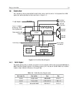
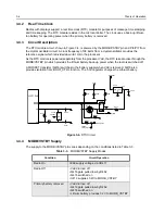
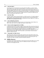
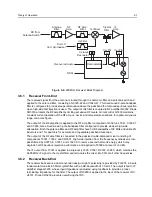
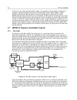
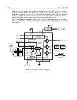
The keypad/PassPort Option Board block diagram is shown in Figure 3-2. The keypad circuitry is
contained on the PassPort Option Board.
Two resistive voltage divider networks form a row and column matrix. Pressing any button
simultaneously grounds a tap on the row and column voltage dividers which outputs a unique row
voltage and column voltage level for that button location. The row and column voltages are applied to
two A/D inputs of the microprocessor (U409 pins 60 and 61). The keypad column voltage is also
applied to a comparator whose threshold is set to produce an interrupt signal (KEY_INT) whenever
any key is pressed. The microprocessor then samples the voltage levels at the keypad row and
keypad column A/D inputs and makes a comparison with a map table to identify the key pressed.
Once the key is identified, a corresponding function is executed.
The LED_EN is set by the codeplug. When the value is set to low, the LED lights up during power up.
A high codeplug setting disables this feature.
Figure 3-2. Keypad/PassPort Option Board Block Diagram
SWB+
Fuse
Low Battery
Detect
Antenna
Switch
PA, Driver
PCIC(ALC)
LI Ion
3.3V
Reg.
Audio
Power
Amplifier
ASFIC_CMP
VCOBIC
FRACTN
LCD
Driver
5V
MECH.
SWB+
UNSWB+
Vdda
Accessories
20 pin Connector
Keypad/Option Board
Vddd
MCU, ROM
and EEPROM
Tx
Led
Control
7.5V
Battery
Vddd
Regulator
Vdda
Regulator
5V
Regulator
On/Off
Switch
RF AMP, IF AMP,
RX/TX Buffers
IFIC
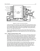
Figure 3-1. DC Power Distribution Block Diagram
40 Pin Connector
Comparator
Keypad
Button
LED
Display
18 Pin
Connector
Key_Int
Keypad Column
Keypad
Row
Data
Содержание HT1250-LS+
Страница 10: ...viii ...
Страница 12: ...x Product Safety and RF Exposure Compliance ...
Страница 16: ...1 4 Introduction ...
Страница 58: ...4 22 Maintenance ...
Страница 64: ...5 6 Schematic Diagrams Overlays and Parts Lists ...
Страница 102: ...5 44 Schematic Diagrams Overlays and Parts Lists Figure 5 34 Keypad PassPort Option Board Schematic Diagram ...


