Theory of Operation
3-9
3.7.2
Fractional-N Synthesizer
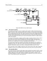
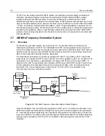
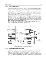
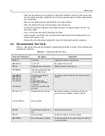
The Fractional-N synthesizer, shown in Figure 3-8, uses a 16.8 MHz reference oscillator (Y3762) to
provide a high stability reference for the system. Stability is better than 2.5 ppm over temperatures of
-30 to 60 °C. Electronic frequency adjustment is achieved by an internal DAC which provides a
frequency adjustment voltage from U3701 pin 25 to the reference oscillator module. The synthesizer
IC U3701 further divides the 16.8 MHz signal (applied to U3701 pin 23) to 2.1 MHz, 2.225 MHz, or 2.4
MHz for use as reference frequencies. It also provides 16.8 MHz at U3701 pin 19 for use by the
ASFIC. A loop filter (C3723-4, R3722-3) removes noise and spurs from the steering voltage applied to
the VCO varactors, with additional filtering located in the VCO circuit.
To achieve fast locking for the synthesizer, an internal adapt charge pump provides higher current at
U3701 pin 45 to quickly force the synthesizer within lock range. The required frequency is then locked
by normal mode charge pump at pin 43. Both the normal and adapt charge pumps get their supply
from the capacitive voltage multiplier made up of C3701-4 and D3701-2. Two 3.3V square waves from
U3701 pins 14-15 provide the drive signals for the voltage multiplier, which generates 13.3V at U3701
pin 47. This voltage is filtered by C3705-6 and C3714.
One of the auxiliary outputs of the synthesizer IC (pin 48) controls transistor switch Q3721 which
outputs a T5 voltage source during transmit and R5 during receive.
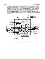
Figure 3-8. 200 MHz Synthesizer Block Diagram
3.7.3
Voltage Controlled Oscillator (VCO)
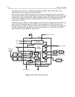
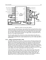
The VCOBIC (U3801), shown in Figure 3-9, in conjunction with the Fractional-N synthesizer (U3701)
generates RF in both the receive and the transmit modes of operation. The TRB line (U3801 pin 19)
determines which oscillator and buffer are enabled. A sample of the RF signal from the enabled
oscillator is routed from U3801 pin 12 through a low pass filter, to the prescaler input of the
synthesizer IC (U3701 pin 32). After frequency comparison in the synthesizer, a resultant DC control
voltage is used to steer the VCO frequency. When the PLL is locked on frequency, this voltage can
DATA
CLK
CEX
MODIN
V
CC
, DC5V
XTAL1
WARP
PREIN
VCP
Reference
Oscillator
Voltage
Multiplier
Voltage
Controlled
Oscillator
2-Pole
Loop Filter
DATA (U409 Pin 100)
CLOCK (U409 Pin 1)
CSX (U409 Pin 2)
MOD IN (U404 Pin 40)
+5V (U3711 Pin 4)
7
8
9
10
13,30
23
25
32
47
VMULT2 VMULT1
BIAS1
SFOUT
AUX3
AUX4
IADAPT
IOUT
GND
FREFOUT
LOCK
4
19
6,22,23,24
43
45
3
2
28
14
15
40
Filtered 5V
Steering
Line
LOCK (U409 Pin 56)
Prescaler In
LO RF
Injection
TX RF
Injection
(First Stage of PA)
FREF (U404 Pin 34)
39
BIAS2
41
48
5V
R5
(U3201 Pin 5)
AUX1
V
DD
, 3.3V
MODOUT
U3701
Low Voltage
Fractional-N
Synthesizer
5,20,34,36
Dual
Transistor
T5
TRB
Содержание HT1250-LS+
Страница 10: ...viii ...
Страница 12: ...x Product Safety and RF Exposure Compliance ...
Страница 16: ...1 4 Introduction ...
Страница 58: ...4 22 Maintenance ...
Страница 64: ...5 6 Schematic Diagrams Overlays and Parts Lists ...
Страница 102: ...5 44 Schematic Diagrams Overlays and Parts Lists Figure 5 34 Keypad PassPort Option Board Schematic Diagram ...


