


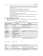


3-16
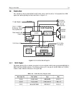
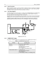
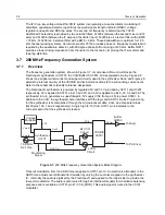
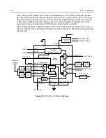
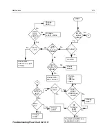
Theory of Operation
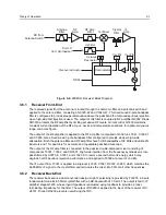
In the transmit mode, Q603 is off and U600-19 is pulled high to 5V by R655, enabling the transmit
VCO and buffer. The 746-794 MHz RF signal from U600 pin 10 is applied as TX_INJ to the input of
the transmitter driver IC (U101 pin 16). TX VCO frequency is determined by ceramic tank resonator
FL601, varactor CR603, and associated components. Audio modulation is superimposed on the
steering line voltage, allowing varactor CR603 to also function as the modulator.
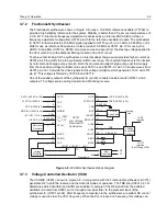
When a high impedance is applied to U3801, pin19, the VCO is operating in battery saver mode. In
this case, both the receive and transmit oscillators as well as the receive transmit and prescaler buffer
are turned off.
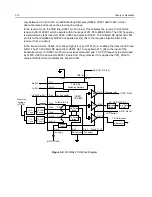
Figure 3-14. 700 MHz VCO Block Diagram
Presc
RX
TX
Matching
Network
Low Pass
Filter
Attenuator
Pin 8
Pin 14
Pin 10
5V
(U201 Pin 28)
VCC Buffers
TX RF Injection
U201 Pin 32
AUX4 (U201 Pin 3)
AUX3 (U201 Pin 2)
Prescaler Out
Pin 12
Pin 19
Pin 20
TX/RX/BS
Switching Network
U600
VCOBIC
Rx Active
Bias
Tx Active
Bias
Pin 2
Rx-I adjust
Pin 1
Tx-I adjust
Pins 9,11,17
Pin 18
Vsens
Circuit
Pin 15
Pin 16
TX VCO
Circuit
TX
Tank
RX VCO
Circuit
RX
Tank
Pin 7
Vcc-Superfilter
Collector/RF in
Pin 4
Pin 5
Pin 6
RX
TX
(U201 Pin 28)
Rx-SW
Tx-SW
Vcc-Logic
(U201 Pin 28)
Steer Line
Voltage
(VCTRL)
Pin 13
Pin 3
TRB_IN
LO RF INJECTION
Level Shifter
Network
Содержание HT1250-LS+
Страница 10: ...viii ...
Страница 12: ...x Product Safety and RF Exposure Compliance ...
Страница 16: ...1 4 Introduction ...
Страница 58: ...4 22 Maintenance ...
Страница 64: ...5 6 Schematic Diagrams Overlays and Parts Lists ...
Страница 102: ...5 44 Schematic Diagrams Overlays and Parts Lists Figure 5 34 Keypad PassPort Option Board Schematic Diagram ...