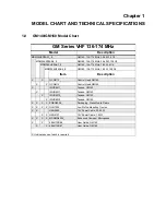
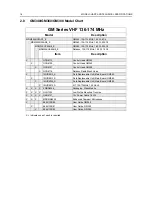
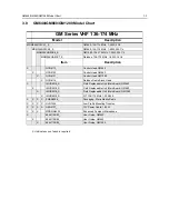
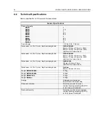


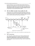


VHF (136-174MHz) Transmitter Power Amplifier (PA) 45 W
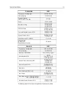
2-9
In order to modulate the PLL, the two spot modulation method is utilized. Via U3201 pin 10
(MODIN), the audio signal is applied to both the A/D converter (low frequency path) as well as the
balance attenuator (high frequency path). The A/D converter changes the low frequency analog
modulating signal into a digital code that is applied to the loop divider, thereby causing the carrier to
deviate. The balance attenuator is used to adjust the VCO’s deviation sensitivity to high frequency
modulating signals. The output of the balance attenuator is present at the MODOUT port (U3201-
41) and connected to the VCO modulation diode D3362 via R3364.
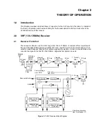
5.0
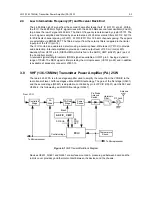
VHF (136-174MHz) Transmitter Power Amplifier (PA) 45 W
The radio’s 45 W PA is a four stage amplifier used to amplify the output from the VCOBIC to the
radio transmit level. The line-up consists of three stages which utilize LDMOS technology, followed
by a final stage using a bipolar device. The gain of the first stage (U3401) is adjustable, controlled by
pin 4 of PCIC (U3501) via Q3501 and Q3502 (VCONT). It is followed by an LDMOS pre-driver stage
(Q3421), an LDMOS driver stage (Q3431) and a bipolar final stage (Q3441).
Figure 5-1
VHF Transmitter Block Diagram
Devices U3401 and Q3421 are surface mounted. The remaining devices are directly attached to the
heat sink.
5.1
Power Controlled Stage
The first stage (U3401) is a 20dB gain integrated circuit containing two LDMOS FET amplifier
stages. It amplifies the RF signal from the VCO (TXINJ). The output power of stage U3401 is
controlled by a DC voltage applied to pin 1 from the power control circuit (U3501 pin 4, with
transistors Q3501 and Q3502 providing current gain and level-shifting). The control voltage
simultaneously varies the bias of two FET stages within U3401. This biasing point determines the
overall gain of U3401 and therefore its output drive level to Q3421, which in turn controls the output
power of the PA.
Antenna
To Microprocessor
P C I C
Pin Diode
Antenna
Switch
RF Jack
Harmonic
Filter
Power
Sense
PA-Final
Stage
PA
Driver
From VCO
Controlled
Stage
Vcontrol
Bias 1
Bias 2
To Microprocessor
Temperature
Sense
SPI BUS
A S F I C _ C M P
PA
PWR
SET
To Microprocessor
Pre
Driver
Содержание 6864115B62-C
Страница 1: ...Professional Radio GM Series Detailed Service Manual 6864115B62 C ...
Страница 2: ...ii ...
Страница 4: ...iv ...
Страница 5: ...Professional Radio GM Series Service Maintainability Issue July 2007 ...
Страница 8: ...ii ...
Страница 22: ...2 10 MAINTENANCE ...
Страница 25: ...Professional Radio GM Series Controlhead Service Information Issue July 2007 ...
Страница 77: ...Professional Radio GM Series Controller Service Information Issue May 2007 ...
Страница 100: ...2 2 TROUBLESHOOTING CHARTS ...
Страница 104: ...3 4 Controller schematics parts list ...
Страница 154: ...3 52 Controller T12 Schematic Diagrams ...
Страница 155: ...Professional Radio GM Series VHF 136 174MHz Service Information Issue May 2007 ...
Страница 164: ...1 6 MODEL CHART AND TECHNICAL SPECIFICATIONS ...
Страница 176: ...2 12 THEORY OF OPERATION ...
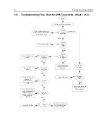
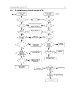
Страница 186: ...3 10 TROUBLESHOOTING CHARTS ...
Страница 190: ...4 4 VHF PCB SCHEMATICS PARTS LISTS ...
Страница 252: ...4 66 VHF 1 25W PCB 8471235L02 Schematics VHF 136 174 MHz IF ...
Страница 256: ...4 70 VHF 1 25W PCB 8471235L02 Schematics ...
Страница 257: ...Professional Radio GM Series UHF 403 470MHz Service Information Issue May 2007 ...
Страница 266: ...1 6 MODEL CHART AND TECHNICAL SPECIFICATIONS ...
Страница 349: ...Professional Radio GM Series LB1 29 6 36 0MHz LB2 36 0 42 0MHz LB3 42 0 50 0MHz Service Information Issue May 2007 ...
Страница 366: ...2 12 THEORY OF OPERATION ...
Страница 372: ...3 6 Low Band TROUBLESHOOTING CHARTS ...
Страница 376: ...4 4 Low band pcb schematics parts lists ...