
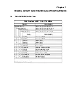
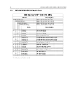
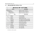
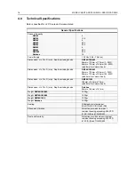
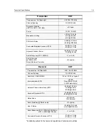


VHF (136-174MHz) Frequency Synthesis
2-7
A voltage of 5V applied to the super filter input (U3201 pin 30) supplies an output voltage of 4.5 VDC
(VSF) at pin 28. It supplies the VCO, VCO modulation bias circuit (via R3363) and the synthesizer
charge pump resistor network (R3251, R3252). The synthesizer supply voltage is provided by the
5V regulator U3211.
In order to generate a high voltage to supply the phase detector (charge pump) output stage at pin
VCP (U3201-47), a voltage of 13 VDC is being generated by the positive voltage multiplier circuitry
(D3201, C3202, C3203). This voltage multiplier is basically a diode capacitor network driven by two
(1.05MHz) 180 degrees out of phase signals (U3201-14 and -15).
Output LOCK (U3201-4) provides information about the lock status of the synthesizer loop. A high
level at this output indicates a stable loop. IC U3201 provides the 16.8 MHz reference frequency at
pin 19.
The serial interface (SRL) is connected to the microprocessor via the data line DATA (U3201-7),
clock line CLK (U3201-8), and chip enable line CSX (U3201-9).
4.3
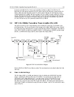
Voltage Controlled Oscillator (VCO)
The Voltage Controlled Oscillator (VCO) consists of the VCO/Buffer IC (VCOBIC, U3301), the TX
and RX tank circuits, the external RX buffer stages, and the modulation circuitry.
Figure 4-1
VHF VCO Block Diagram
Presc
RX
TX
Matching
Network
Low Pass
Filter
Attenuator
Pin8
Pin14
Pin10
(U3211 Pin1)
VCC Buffers
TX RF Injection
U3201 Pin 32
AUX3 (U3201 Pin2)
Prescaler Out
Pin 12
Pin 19
Pin 20
TX/RX/BS
Switching Network
U3301
VCOBIC
Rx
Active Bias
Tx
Active Bias
Pin2
Rx-I adjust
Pin1
Tx-I adjust
Pins 9,11,17
Pin18
Vsens
Circuit
Pin15
Pin16
RX VCO
Circuit
TX VCO
Circuit
RX Tank
TX Tank
Pin7
Vcc-Superfilter
Collector/RF in
Pin4
Pin5
Pin6
RX
TX
(U3201 Pin28)
Rx-SW
Tx-SW
Vcc-Logic
(U3211 Pin1)
Steer Line
Voltage
(VCTRL)
Pin13
Pin3
TRB IN
LO RF INJECTION
Q3304
Q3301
Содержание 6864115B62-C
Страница 1: ...Professional Radio GM Series Detailed Service Manual 6864115B62 C ...
Страница 2: ...ii ...
Страница 4: ...iv ...
Страница 5: ...Professional Radio GM Series Service Maintainability Issue July 2007 ...
Страница 8: ...ii ...
Страница 22: ...2 10 MAINTENANCE ...
Страница 25: ...Professional Radio GM Series Controlhead Service Information Issue July 2007 ...
Страница 77: ...Professional Radio GM Series Controller Service Information Issue May 2007 ...
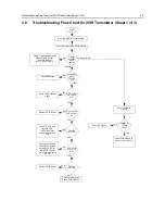
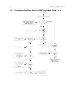
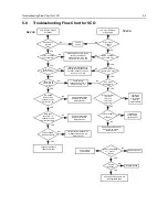
Страница 100: ...2 2 TROUBLESHOOTING CHARTS ...
Страница 104: ...3 4 Controller schematics parts list ...
Страница 154: ...3 52 Controller T12 Schematic Diagrams ...
Страница 155: ...Professional Radio GM Series VHF 136 174MHz Service Information Issue May 2007 ...
Страница 164: ...1 6 MODEL CHART AND TECHNICAL SPECIFICATIONS ...
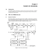
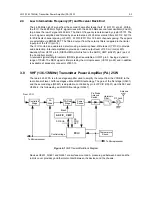
Страница 176: ...2 12 THEORY OF OPERATION ...
Страница 186: ...3 10 TROUBLESHOOTING CHARTS ...
Страница 190: ...4 4 VHF PCB SCHEMATICS PARTS LISTS ...
Страница 252: ...4 66 VHF 1 25W PCB 8471235L02 Schematics VHF 136 174 MHz IF ...
Страница 256: ...4 70 VHF 1 25W PCB 8471235L02 Schematics ...
Страница 257: ...Professional Radio GM Series UHF 403 470MHz Service Information Issue May 2007 ...
Страница 266: ...1 6 MODEL CHART AND TECHNICAL SPECIFICATIONS ...
Страница 349: ...Professional Radio GM Series LB1 29 6 36 0MHz LB2 36 0 42 0MHz LB3 42 0 50 0MHz Service Information Issue May 2007 ...
Страница 366: ...2 12 THEORY OF OPERATION ...
Страница 372: ...3 6 Low Band TROUBLESHOOTING CHARTS ...
Страница 376: ...4 4 Low band pcb schematics parts lists ...