MDDR Subsystem
Microsemi Proprietary UG0446 User Guide Revision 7.0
75
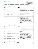
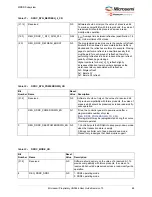
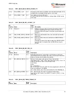
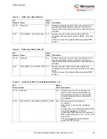
[15:0]
REG_DDRC_MR
0×095A Value to be loaded into the DRAM Mode register. Bit 8 is for
the DLL and the setting here is ignored. The controller sets
appropriately. During DRAM initialization procedure, the
controller will send the mode register setting to DRAM. The
mode register sets the DRAM burst length, burst type, CAS
latency (CL), and operating mode.
Table 43 •
DDRC_INIT_EMR_CR
Bit
Number
Name
Reset
Value
Description
[31:16]
Reserved
0×0
Software should not rely on the value of a reserved bit. To
provide compatibility with future products, the value of a
reserved bit should be preserved across a read-modify-write
operation.
[15:0]
REG_DDRC_EMR
0×0402 Value to be loaded into DRAM EMR registers. Bits [9:7] are
for OCD and the setting in this bits is ignored.
The controller sets those bits appropriately.
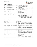
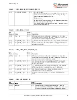
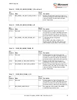
Table 44 •
DDRC_INIT_EMR2_CR
Bit
Number
Name
Reset
Value
Description
[31:16]
Reserved
0×0
Software should not rely on the value of a reserved bit. To provide
compatibility with future products, the value of a reserved bit should be
preserved across a read-modify-write operation.
[15:0]
REG_DDRC_EMR2
0×0
Value to be loaded into DRAM EMR2 registers.
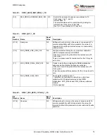
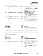
Table 45 •
DDRC_INIT_EMR3_CR
Bit
Number
Name
Reset
Value
Description
[31:16]
Reserved
0×0
Software should not rely on the value of a reserved bit. To provide
compatibility with future products, the value of a reserved bit should be
preserved across a read-modify-write operation.
[15:0]
REG_DDRC_EMR3
0×0
Value to be loaded into DRAM EMR3 registers.
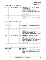
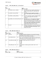
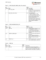
Table 46 •
DDRC_DRAM_BANK_TIMING_PARAM_CR
Bit
Number
Name
Reset
Value
Description
[31:12]
Reserved
0×0
Software should not rely on the value of a reserved bit. To provide
compatibility with future products, the value of a reserved bit should be
preserved across a read-modify-write operation.
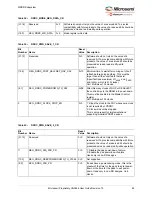
Table 42 •
DDRC_INIT_MR_CR

