3. TECHNICAL BRIEF
- 52 -
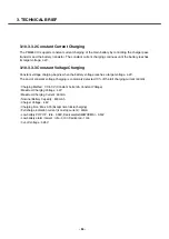
3.10.3.3 Charging control
A programmable charging block in PM6650 is used for battery charging. It is possible to set limits for
the charging current. The external supply typically connects directly to pin (VCHG). The voltage on this
pin (VCHG) is monitored by detection circuitry to ascertain whether a valid external supply is applied or
not. For additional accuracy or to capture variations over time, this voltage is routed internally to the
housekeeping ADC via the analog multiplexer. PM6650 circuits monitor voltages at VCHARGER and
ICHARGE pins to determine which supply should be used and when to switch between the two
supplies. These pins are connected to the Source (or emitter) and Drain (or collector) contacts of the
pass transistor respectively.
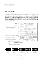
U8500 Battery Bar Display(Stand By Condition)
4.2V~3.82V
100~75 (%)
3.81V~3.75V
75~50 (%)
3.74V~3.68V
50~25 (%)
3.67V~3.51V
25~2 (%)
3.50V~3.28V
2~0 (%)
Содержание U8500
Страница 1: ...Date February 2006 Issue 1 0 Service Manual Model U8500 Service Manual U8500 ...
Страница 20: ...3 TECHNICAL BRIEF 21 ...
Страница 32: ...3 TECHNICAL BRIEF 33 Figure 3 5 6 1 GSM PA functional block diagram ...
Страница 35: ...3 TECHNICAL BRIEF 36 Figure 3 5 10 1 Bluetooth system architecture ...
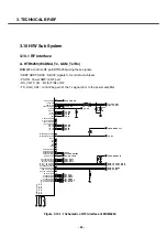
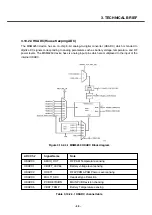
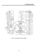
Страница 50: ...3 TECHNICAL BRIEF 51 Figure 3 10 3 2 1 PM6650 Functional Block Diagram ...
Страница 110: ...4 TROUBLE SHOOTING 111 R605 R606 receiver signal serial resistor Receiver CN600 50pin LCD connector FPCB for LCD Module ...
Страница 112: ...4 TROUBLE SHOOTING 113 R605 R606 receiver signal serial resistor CN600 50pin LCD connector CN901 C907 C911 ...
Страница 114: ...4 TROUBLE SHOOTING 115 Loud Speaker U502 U503 Amp ...
Страница 118: ...4 TROUBLE SHOOTING 119 C200 C201 for MIC serial capacitor ...
Страница 121: ...4 TROUBLE SHOOTING 122 Q404 Q403 Q402 VBATT GND ...
Страница 128: ...5 DOWNLOAD 129 5 Choose a Module Image file after clicking on the Browse button U8500 U8500 U8500 U8500 U8500 U8500 ...
Страница 132: ...5 DOWNLOAD 133 Downloading the AMSS Modem image Rebooting and waiting for a while Performing NV restore ...
Страница 134: ...5 DOWNLOAD 135 Download of Module image in progress Download process has completed successfully ...
Страница 143: ...6 BLOCK DIAGRAM 144 6 3 Interface Diagram U8500 Interface Diagram ...
Страница 145: ... 146 ...
Страница 154: ... 155 U8500 8 PCB LAYOUT ...
Страница 155: ... 156 8 PCB LAYOUT U8500 ...
Страница 156: ... 157 8 PCB LAYOUT ...
Страница 157: ... 158 8 PCB LAYOUT ...
Страница 158: ... 159 U8500 8 PCB LAYOUT ...
Страница 159: ... 160 U8500 8 PCB LAYOUT ...
Страница 166: ...9 CALIBRATION 167 Click START button U8500 U8500_ver1 1 U8500 U8500 Click U8500 ...
Страница 167: ... 168 ...
Страница 169: ... 170 ...
Страница 194: ...Note ...
Страница 195: ...Note ...

