3. TECHNICAL BRIEF
- 50 -
3.10.3 Power Block
3.10.3.1 General
MSM6250, included RF, is fully covered by PM6650(Qualcomm PMIC). PM6650 cover the power of
MSM6250, MSM memory, RF block, Bluetooth, Trans flash, USIM and TCXO.
Major power components are :
PM6650(U402)
: Phone power supply
BH28FB1WHFV(U411)
: LCD Power supply
QST4(Q403,Q404)
: External charger supply switching
SI3493DV (Q402)
: Main Battery charging control
SI8402DB,SI8407DB(Q400,Q401)
: WCDMA PAM power selection control
MIC2211(U501)
: Camera power supply
3.10.3.2 PM6650
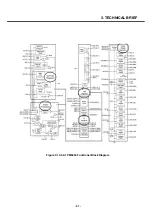
The PM6650 device integrates all wireless handset power management. The power management
portion accepts power from all the most common sources - battery, external charger, adapter, coin cell
back-up - and generates all the regulated voltages needed to power the appropriate handset
electronics. It monitors and controls the power sources, detecting which sources are applied, verifying
that they are within acceptable operational limits, and coordinates battery and coin cell recharging
while maintaining the handset electronics supply voltages. Eight programmable output voltages are
generated using low dropout voltage regulators, all derived from a common trimmed voltage reference.
A dedicated controller manages the TCXO warm-up and signal buffering, and key parameters (under-
voltage lockout and crystal oscillator signal presence) are monitored to protect against detrimental
conditions.
MSM device controls and statuses the PM6650 IC using a three-line Serial Bus Interface (SBI)
supplemented by an Interrupt Manager for time-critical information. Another dedicated IC Interface
circuit monitors multiple trigger events and controls the power-on sequence.
Содержание U8500
Страница 1: ...Date February 2006 Issue 1 0 Service Manual Model U8500 Service Manual U8500 ...
Страница 20: ...3 TECHNICAL BRIEF 21 ...
Страница 32: ...3 TECHNICAL BRIEF 33 Figure 3 5 6 1 GSM PA functional block diagram ...
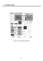
Страница 35: ...3 TECHNICAL BRIEF 36 Figure 3 5 10 1 Bluetooth system architecture ...
Страница 50: ...3 TECHNICAL BRIEF 51 Figure 3 10 3 2 1 PM6650 Functional Block Diagram ...
Страница 110: ...4 TROUBLE SHOOTING 111 R605 R606 receiver signal serial resistor Receiver CN600 50pin LCD connector FPCB for LCD Module ...
Страница 112: ...4 TROUBLE SHOOTING 113 R605 R606 receiver signal serial resistor CN600 50pin LCD connector CN901 C907 C911 ...
Страница 114: ...4 TROUBLE SHOOTING 115 Loud Speaker U502 U503 Amp ...
Страница 118: ...4 TROUBLE SHOOTING 119 C200 C201 for MIC serial capacitor ...
Страница 121: ...4 TROUBLE SHOOTING 122 Q404 Q403 Q402 VBATT GND ...
Страница 128: ...5 DOWNLOAD 129 5 Choose a Module Image file after clicking on the Browse button U8500 U8500 U8500 U8500 U8500 U8500 ...
Страница 132: ...5 DOWNLOAD 133 Downloading the AMSS Modem image Rebooting and waiting for a while Performing NV restore ...
Страница 134: ...5 DOWNLOAD 135 Download of Module image in progress Download process has completed successfully ...
Страница 143: ...6 BLOCK DIAGRAM 144 6 3 Interface Diagram U8500 Interface Diagram ...
Страница 145: ... 146 ...
Страница 154: ... 155 U8500 8 PCB LAYOUT ...
Страница 155: ... 156 8 PCB LAYOUT U8500 ...
Страница 156: ... 157 8 PCB LAYOUT ...
Страница 157: ... 158 8 PCB LAYOUT ...
Страница 158: ... 159 U8500 8 PCB LAYOUT ...
Страница 159: ... 160 U8500 8 PCB LAYOUT ...
Страница 166: ...9 CALIBRATION 167 Click START button U8500 U8500_ver1 1 U8500 U8500 Click U8500 ...
Страница 167: ... 168 ...
Страница 169: ... 170 ...
Страница 194: ...Note ...
Страница 195: ...Note ...

