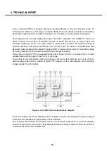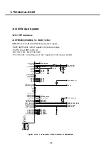
A low current (VCONT) pin provides improved operating efficiency in the low RF power range. To
further improve efficiency in this range, a separate VBIAS pin can be directly connected to the battery,
which allows reducing VCC1 and VCC2 voltages to 0.8 V to achieve very low power consumption.
The single Gallium Arsenide (GaAs) Microwave Monolithic Integrated Circuit (MMIC) contains all
active circuitry in the module. The MMIC contains on-board bias circuitry, as well as input and
interstage matching circuits. The output match is realized off-chip within the module package to
optimize efficiency and power performance into a 50 Ω load. This device is manufactured with
Skyworks’ GaAs Heterojunction Bipolar Transistor (HBT) process that provides for all positive voltage
DC supply operation while maintaining high efficiency and good linearity.
Primary bias to the SKY77410 is supplied directly from a three-cell Ni-Cd, a singlecell Li-Ion, or other
suitable battery with an output in the 3.2 to 4.2 volt range.
Power down is accomplished by setting the voltage on the low current reference pin to zero volts. No
external supply side switch is needed as typical “off” leakage is a few microamperes with full primary
voltage supplied from the battery.
An isolator between the Power Amplifier and the duplexer is highly recommended to provide constant
load and source impedances (respectively) to those devices.
This improves PA stability, ACPR performance, and harmonic suppression, as well as duplexer
isolation, insertion loss, and ripple. Transmitter performance is always improved when an isolator is
included and is well worth the added cost.
3. TECHNICAL BRIEF
- 30 -
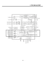
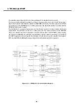
Figure 3.5.3-1 UMTS PA functional block diagram
Содержание U8500
Страница 1: ...Date February 2006 Issue 1 0 Service Manual Model U8500 Service Manual U8500 ...
Страница 20: ...3 TECHNICAL BRIEF 21 ...
Страница 32: ...3 TECHNICAL BRIEF 33 Figure 3 5 6 1 GSM PA functional block diagram ...
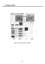
Страница 35: ...3 TECHNICAL BRIEF 36 Figure 3 5 10 1 Bluetooth system architecture ...
Страница 50: ...3 TECHNICAL BRIEF 51 Figure 3 10 3 2 1 PM6650 Functional Block Diagram ...
Страница 110: ...4 TROUBLE SHOOTING 111 R605 R606 receiver signal serial resistor Receiver CN600 50pin LCD connector FPCB for LCD Module ...
Страница 112: ...4 TROUBLE SHOOTING 113 R605 R606 receiver signal serial resistor CN600 50pin LCD connector CN901 C907 C911 ...
Страница 114: ...4 TROUBLE SHOOTING 115 Loud Speaker U502 U503 Amp ...
Страница 118: ...4 TROUBLE SHOOTING 119 C200 C201 for MIC serial capacitor ...
Страница 121: ...4 TROUBLE SHOOTING 122 Q404 Q403 Q402 VBATT GND ...
Страница 128: ...5 DOWNLOAD 129 5 Choose a Module Image file after clicking on the Browse button U8500 U8500 U8500 U8500 U8500 U8500 ...
Страница 132: ...5 DOWNLOAD 133 Downloading the AMSS Modem image Rebooting and waiting for a while Performing NV restore ...
Страница 134: ...5 DOWNLOAD 135 Download of Module image in progress Download process has completed successfully ...
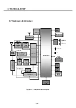
Страница 143: ...6 BLOCK DIAGRAM 144 6 3 Interface Diagram U8500 Interface Diagram ...
Страница 145: ... 146 ...
Страница 154: ... 155 U8500 8 PCB LAYOUT ...
Страница 155: ... 156 8 PCB LAYOUT U8500 ...
Страница 156: ... 157 8 PCB LAYOUT ...
Страница 157: ... 158 8 PCB LAYOUT ...
Страница 158: ... 159 U8500 8 PCB LAYOUT ...
Страница 159: ... 160 U8500 8 PCB LAYOUT ...
Страница 166: ...9 CALIBRATION 167 Click START button U8500 U8500_ver1 1 U8500 U8500 Click U8500 ...
Страница 167: ... 168 ...
Страница 169: ... 170 ...
Страница 194: ...Note ...
Страница 195: ...Note ...


