3. TECHNICAL BRIEF
- 23 -
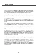
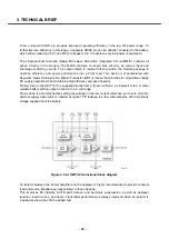
The waveform at the dual Tx VCO output is the GMSK-modulated signal centered at the desired GSM
channel frequency. A phase-locked loop circuit is used to translate the GMSK-modulated signal from IF
to RF primarily for two reasons:
1. Phase-locked loops provide a lowpass filter function from the reference input to the VCO output. This
results in a bandpass function centered at the desired channel frequency that provides steep, well-
controlled rejection of the out-of-band spectrum.
2. The resulting output bandpass function is virtually unchanged as the transmitter is tuned over
channels spanning the GSM operating band.
The PA is a key component in any transmitter chain and must complement the rest of the transmitter
precisely. For GSM band operation, the closed-loop transmit power control functions add even more
requirements relative to the UMTS PA. In addition to gain control and switching requirements, the usual
RF parameters such as gain, output power level, several output spectrum requirements, and power
supply current are critical. The gain must be sufficient and variable to deliver the desired transmitter
output power given the VCO output level, the subsequent passive devices’ losses, and the control set
point. The maximum and minimum transmitter output power levels depend upon the operating band
class and mobile station class per the applicable standard. Transmitter timing requirements and inband
and out-of-band emissions, all dominated by the PA, are also specified by the applicable standard.
The active dual Tx VCO output is applied to the dual power amplifier to continue the transmit path, and
feedback to the RTR6250 IC to complete the frequency control loop. The PA operating band (EGSM or
DCS/PCS) is selected by the MSM device GPIO control (GSM_PA_BAND).
3.3 WCDMA Mode
3.3.1 Receiver
The UMTS duplexer receiver output is routed to LNA circuits within the RFR6250 IC. The LNA gain is
dynamically controlled by the MSM6250 IC to cover full receiver dynamic range and to save current
consumption.
The UMTS LNA output is routed to the down conversion mixer inputs, in the RFR6250 IC, through a
band selection filter that transforms a single-ended 50-Ω source to differential 100-Ω load impedance
that is matched to the RFR6250 IC. The RFR input uses a differential configuration to improve second-
order inter-modulation and common mode rejection performance. The RFR6250 IC input stages
include MSMcontrolled gain adjustments that further extend receiver dynamic range.
Содержание U8500
Страница 1: ...Date February 2006 Issue 1 0 Service Manual Model U8500 Service Manual U8500 ...
Страница 20: ...3 TECHNICAL BRIEF 21 ...
Страница 32: ...3 TECHNICAL BRIEF 33 Figure 3 5 6 1 GSM PA functional block diagram ...
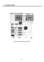
Страница 35: ...3 TECHNICAL BRIEF 36 Figure 3 5 10 1 Bluetooth system architecture ...
Страница 50: ...3 TECHNICAL BRIEF 51 Figure 3 10 3 2 1 PM6650 Functional Block Diagram ...
Страница 110: ...4 TROUBLE SHOOTING 111 R605 R606 receiver signal serial resistor Receiver CN600 50pin LCD connector FPCB for LCD Module ...
Страница 112: ...4 TROUBLE SHOOTING 113 R605 R606 receiver signal serial resistor CN600 50pin LCD connector CN901 C907 C911 ...
Страница 114: ...4 TROUBLE SHOOTING 115 Loud Speaker U502 U503 Amp ...
Страница 118: ...4 TROUBLE SHOOTING 119 C200 C201 for MIC serial capacitor ...
Страница 121: ...4 TROUBLE SHOOTING 122 Q404 Q403 Q402 VBATT GND ...
Страница 128: ...5 DOWNLOAD 129 5 Choose a Module Image file after clicking on the Browse button U8500 U8500 U8500 U8500 U8500 U8500 ...
Страница 132: ...5 DOWNLOAD 133 Downloading the AMSS Modem image Rebooting and waiting for a while Performing NV restore ...
Страница 134: ...5 DOWNLOAD 135 Download of Module image in progress Download process has completed successfully ...
Страница 143: ...6 BLOCK DIAGRAM 144 6 3 Interface Diagram U8500 Interface Diagram ...
Страница 145: ... 146 ...
Страница 154: ... 155 U8500 8 PCB LAYOUT ...
Страница 155: ... 156 8 PCB LAYOUT U8500 ...
Страница 156: ... 157 8 PCB LAYOUT ...
Страница 157: ... 158 8 PCB LAYOUT ...
Страница 158: ... 159 U8500 8 PCB LAYOUT ...
Страница 159: ... 160 U8500 8 PCB LAYOUT ...
Страница 166: ...9 CALIBRATION 167 Click START button U8500 U8500_ver1 1 U8500 U8500 Click U8500 ...
Страница 167: ... 168 ...
Страница 169: ... 170 ...
Страница 194: ...Note ...
Страница 195: ...Note ...

