3. TECHNICAL BRIEF
- 41 -
3.8.6 Wideband CODEC
The MSM6250 device integrates a wideband voice/audio CODEC into the mobile station modem
(MSM). The CODEC supports two differential microphone inputs, one differential earphone output, one
single-ended earphone output, and a differential analog auxiliary interface on two single-ended
earphone output. The CODEC integrates the microphone and earphone amplifiers into the MSM6250
device, reducing the external component count to just a few passive components.
The microphone (Tx) audio path consists of a two-stage amplifier with the gain of the second stage set
externally. The Rx/Tx paths are designed to meet the ITU-G.712 requirements for digital transmission
systems.
3.8.7 Vocoder Subsystem
The MSM6250 device’s QDSP4000 supports AMR vocoder. In addition, the QDSP4000 has modules
to support the following audio functions: DTMF tone generation, DTMF tone detection, Tx/Rx volume
controls, Tx/Rx automatic gain control (AGC), Rx Automatic Volume Control (AVC), EarSeal Echo
Canceller (ESEC), Acoustic Echo Canceller (AEC), Noise Suppression (NS), and programmable, 13-
tap, Type-I, FIR, Tx/Rx compensation filters. The MSM6200 device’s integrated ARM7TDMI processor
downloads the firmware into the QDSP4000 and configures QDSP4000 to support the desired
functionality.
3.8.8 HKADC
TheMSM6250 device has an on-chip 8-bit analog-to-digital converter (ADC) which is intended to
digitize DC signals corresponding to analog parameters such as battery voltage, temperature, and RF
power levels. The MSM6250 device has six analog input pins which are multiplexed to the input of the
internal HKADC.
3.8.9 General-Purpose Input/Output Interface
The MSM6250 device has general-purpose bidirectional input/output pins. Some of the GPIO pins
have alternate functions supported on them. The alternate functions include USB interface, additional
RAM, ROM, general-purpose chip selects, parallel LCD interface, and UART interface.
Содержание U8500
Страница 1: ...Date February 2006 Issue 1 0 Service Manual Model U8500 Service Manual U8500 ...
Страница 20: ...3 TECHNICAL BRIEF 21 ...
Страница 32: ...3 TECHNICAL BRIEF 33 Figure 3 5 6 1 GSM PA functional block diagram ...
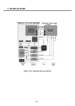
Страница 35: ...3 TECHNICAL BRIEF 36 Figure 3 5 10 1 Bluetooth system architecture ...
Страница 50: ...3 TECHNICAL BRIEF 51 Figure 3 10 3 2 1 PM6650 Functional Block Diagram ...
Страница 110: ...4 TROUBLE SHOOTING 111 R605 R606 receiver signal serial resistor Receiver CN600 50pin LCD connector FPCB for LCD Module ...
Страница 112: ...4 TROUBLE SHOOTING 113 R605 R606 receiver signal serial resistor CN600 50pin LCD connector CN901 C907 C911 ...
Страница 114: ...4 TROUBLE SHOOTING 115 Loud Speaker U502 U503 Amp ...
Страница 118: ...4 TROUBLE SHOOTING 119 C200 C201 for MIC serial capacitor ...
Страница 121: ...4 TROUBLE SHOOTING 122 Q404 Q403 Q402 VBATT GND ...
Страница 128: ...5 DOWNLOAD 129 5 Choose a Module Image file after clicking on the Browse button U8500 U8500 U8500 U8500 U8500 U8500 ...
Страница 132: ...5 DOWNLOAD 133 Downloading the AMSS Modem image Rebooting and waiting for a while Performing NV restore ...
Страница 134: ...5 DOWNLOAD 135 Download of Module image in progress Download process has completed successfully ...
Страница 143: ...6 BLOCK DIAGRAM 144 6 3 Interface Diagram U8500 Interface Diagram ...
Страница 145: ... 146 ...
Страница 154: ... 155 U8500 8 PCB LAYOUT ...
Страница 155: ... 156 8 PCB LAYOUT U8500 ...
Страница 156: ... 157 8 PCB LAYOUT ...
Страница 157: ... 158 8 PCB LAYOUT ...
Страница 158: ... 159 U8500 8 PCB LAYOUT ...
Страница 159: ... 160 U8500 8 PCB LAYOUT ...
Страница 166: ...9 CALIBRATION 167 Click START button U8500 U8500_ver1 1 U8500 U8500 Click U8500 ...
Страница 167: ... 168 ...
Страница 169: ... 170 ...
Страница 194: ...Note ...
Страница 195: ...Note ...

