The off-chip loop filter allows optimization of key PLL performance characteristics (stability, transitory
response, settling time, and phase noise) for different applications. Guidelines are provided in the next
subsection for proper implementation of this critical circuit.
3.5 Off-chip RF Components
3.5.1 Front End Module(U1006)
Front End module integrates antenna switch module and GSM Rx filter.
The antenna switch module allows multiple operating bands and modes to share the same antenna. In
the U8500 design, a common antenna connects to one of six paths: 1) UMTS-2100 Rx/Tx, 2) EGSM
Rx, 3) DCS-1800 Rx, 4) PCS-1900 Rx, 5)EGSM Tx, and 6) DCS-1800, PCS-1900 Tx. UMTS
operation requires simultaneous reception and transmission, so the UMTS Rx/Tx connection is routed
to a duplexer that separates receive and transmit signals. GSM band of operation is time division
duplexed, so only the receiver or transmitter is active at any time and a frequency duplexer is not
required. The module includes lowpass filters for the GSM bands transmit paths to reduce out-of-band
emissions, PA harmonics in particular.
The GSM mode RF filters are located before their LNAs, so their insertion losses are extremely critical
(1.5 dB typical). Other important parameters are:
• Out-of-band rejection or attenuation levels
- Far out-of-band signals - ranging from DC up to the first band of particular concern and from the
last band of particular concern to beyond three times the highest passband frequency.
- Frequencies of particular concern . bands known to include other wireless transmitters that may
deliver significant power levels to the receiver input.
- GSM band receivers operate while the handset transmitters are off so there are no Tx-band
leakage attenuation requirements.
• Phase and amplitude balance - the UMTS discussion presented above applies for GSM bands as
well. See the data sheet for specific values. Of course, passband ripple and return loss are still
important in all cases for the same reasons explained in the antenna switch module and duplexer
sections.
3. TECHNICAL BRIEF
- 28 -
Содержание U8500
Страница 1: ...Date February 2006 Issue 1 0 Service Manual Model U8500 Service Manual U8500 ...
Страница 20: ...3 TECHNICAL BRIEF 21 ...
Страница 32: ...3 TECHNICAL BRIEF 33 Figure 3 5 6 1 GSM PA functional block diagram ...
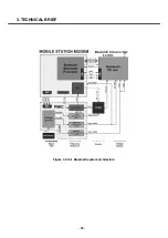
Страница 35: ...3 TECHNICAL BRIEF 36 Figure 3 5 10 1 Bluetooth system architecture ...
Страница 50: ...3 TECHNICAL BRIEF 51 Figure 3 10 3 2 1 PM6650 Functional Block Diagram ...
Страница 110: ...4 TROUBLE SHOOTING 111 R605 R606 receiver signal serial resistor Receiver CN600 50pin LCD connector FPCB for LCD Module ...
Страница 112: ...4 TROUBLE SHOOTING 113 R605 R606 receiver signal serial resistor CN600 50pin LCD connector CN901 C907 C911 ...
Страница 114: ...4 TROUBLE SHOOTING 115 Loud Speaker U502 U503 Amp ...
Страница 118: ...4 TROUBLE SHOOTING 119 C200 C201 for MIC serial capacitor ...
Страница 121: ...4 TROUBLE SHOOTING 122 Q404 Q403 Q402 VBATT GND ...
Страница 128: ...5 DOWNLOAD 129 5 Choose a Module Image file after clicking on the Browse button U8500 U8500 U8500 U8500 U8500 U8500 ...
Страница 132: ...5 DOWNLOAD 133 Downloading the AMSS Modem image Rebooting and waiting for a while Performing NV restore ...
Страница 134: ...5 DOWNLOAD 135 Download of Module image in progress Download process has completed successfully ...
Страница 143: ...6 BLOCK DIAGRAM 144 6 3 Interface Diagram U8500 Interface Diagram ...
Страница 145: ... 146 ...
Страница 154: ... 155 U8500 8 PCB LAYOUT ...
Страница 155: ... 156 8 PCB LAYOUT U8500 ...
Страница 156: ... 157 8 PCB LAYOUT ...
Страница 157: ... 158 8 PCB LAYOUT ...
Страница 158: ... 159 U8500 8 PCB LAYOUT ...
Страница 159: ... 160 U8500 8 PCB LAYOUT ...
Страница 166: ...9 CALIBRATION 167 Click START button U8500 U8500_ver1 1 U8500 U8500 Click U8500 ...
Страница 167: ... 168 ...
Страница 169: ... 170 ...
Страница 194: ...Note ...
Страница 195: ...Note ...

