(No.RA020<Rev.002>)1-99
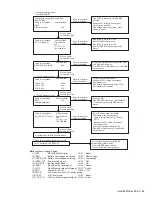
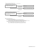
[The MPU/DSP IC is abnormal]
Replace the PCB.
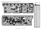
Check the Main unit PCB.
[The 18BT_HCI TX (RXD2)
line circuit is faulty]
Visual check of the CP1, IC6, R22
(Whether not damaged)
Replace any abnormal parts.
When an abnormal
condition is confirmed.
When a normal
condition is confirmed.
From connector to SAW: CN5, C40, R24, R23
SAW parts : L9(side A), D17, D18
GPS IC RF Matching parts(side A) : C38, C36, L7
Verify the RF input circuit for the GPS.
SAW, GPS IC RF Matching parts
[The GPS RF input circuit is faulty]
Replace the GPS RF input circuit
parts. (only the parts which can be
replaced.) If any unexchangeable
parts are abnormal, replace the PCB.
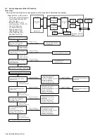
Verify the BT/GPS control signal
(BTMF_nSHUTDoWN).
IC1 (5 pin): 1.8V
Verify the BT/GPS control
signal (BT/_SHUTDOWN).
CN1 (14 pin): 3.3V
Verify the BT/GPS control
signal (18BT_RX).
IC6 (7 pin):
Square waveform UART data
of 1.8V logic.
Baud rate:
Default: 115.2Kbps
After: 3.967Mbps.
[The BT/GPS power supply
line 33GPS circuit is faulty]
C23, C24, R15, C25, R16, IC4, C7,
R19, C26, C27, C29, L2, R14, C3
Replace any abnormal parts.
Check the Main unit PCB.
Check the Main unit PCB.
Check the Main unit PCB.
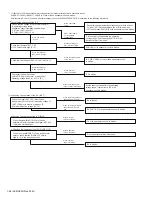
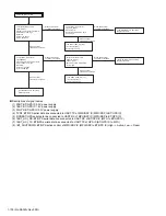
[/BT_SHUTDOWN line circuit
is faulty]
Visual check of the IC1, R7
(Whether not damaged)
Replace any abnormal parts.
Verify the BT/GPS control
signal (TXD2).
CN1 (6 pin):
Square waveform UART data
of 3.3V logic.
[The 18BT_HC1 RX (TXD2)
line circuit is faulty]
Visual check of the CP1, IC6, R22
(Whether not damaged)
Replace any abnormal parts.
Verify the BT/GPS control
signal (18BT_TX).
IC6 (8 pin):
Square waveform UART data
of 1.8V logic.
Verify the BT/GPS control
signal (RXD2).
CN1(7 pin): Square waveform
UART data of 3.3V logic.
Baud rate:
Default: 115.2kbps
After: 3.967Mbps.
When an abnormal
condition is confirmed.
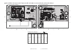
Check the Module (BT/GPS) unit PCB side B.
Verify the BT/GPS power
supply.
(33GPS) L6: 3.3V
Verify the power supply voltage
after removing the KRA-40.
(33GPS) L6: 3.3V
[The KRA-40 may be broken]
Replace the KRA-40.
When an abnormal
condition is confirmed.
When a normal
condition is confirmed.
Verify the power supply voltage
and the BT/GPS control signal.
CN1 (1 pin, 2 pin) : 5.4V
CN1 (16 pin) : 3.3V
Check the Main unit PCB.
When an abnormal
condition is confirmed.
When an abnormal
condition is confirmed.
When an abnormal
condition is confirmed.
When an abnormal
condition is confirmed.
When an abnormal
condition is confirmed.
When an abnormal
condition is confirmed.
When an abnormal
condition is confirmed.
When a normal
condition is confirmed.
When a normal
condition is confirmed.
When a normal
condition is confirmed.
When a normal
condition is confirmed.
When a normal
condition is confirmed.
When a normal
condition is confirmed.
When a normal
condition is confirmed.
When an abnormal
r
condition is confirmed.
When an abnormal
r
condition is confirmed.
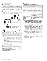
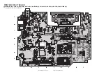
Visual check of the PCB side B parts
(Whether not damaged).
Visual check the following parts.
Содержание NX-5700
Страница 106: ...MEMO ...
Страница 137: ...MEMO ...
Страница 138: ... No RA020 Rev 002 VSE Printed in Japan JVC KENWOOD Corporation Communications Systems Business Unit ...


