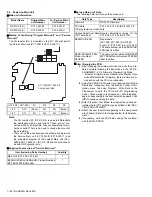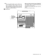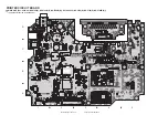
(No.RA020<Rev.002>)1-95
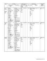
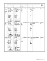
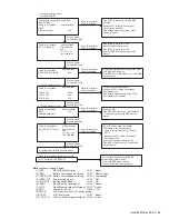
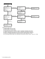
The LCD displays control
The LCD displays control
When an error display appears on the LCD.
If the /FRST is always 0V, the MPU/DSP
is broken.
Remove D701 to check the voltage of
Flash memory side R732.
If the voltage becomes abnormal, Flash
memory is broken.
Points to be checked
Normal voltage
/CS_FIC704(4 pin)
After power-on,
and
If the IC704 (1 pin) is 0V or 1.8V,
the MPU/DSP may be broken.
If the IC704 (2 pin) is 0V or 1.8V,
the MPU/DSP or Flash memory may be
broken.
Points to be checked
Normal voltage
SBC MPU/DSP side R51
3.3V
1.8V
Points to be checked
Normal voltage
54M C841
5.36V
18M C839
1.8V
33M C820
3.3V
The BGA parts are not broken.
Remove the FFC of Main unit between
Sub (Display) unit.
If the voltage becomes normal, the FFC or
Sub (Display) unit is broken.
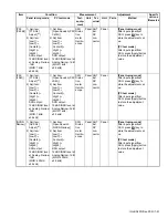
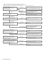
The LCD displays “INIT ERROR 1”.
An error occurs when the mobile DDR
internal RAM reads or writes.
The mobile DDR may be broken.
Check the flowchart from beginning.
Points to be checked
Normal voltage
PRST
3.3V
Remove Q703.
If the MPU/DSP side is 3.3V, the MPU/DSP
or Flash memory or mobile DDR may be
broken.
Points to be checked
Normal voltage
/CS_LCD CP717 (8 pin)
After power-on
and
/CS_LCD has an abnormal voltage.
Check each of the following items.
Check to see the terminal of L731 and
CP717.
Remove the FFC of Main unit between
Sub (Display) unit.
As a result, if the abnormality yet, the
MPU/DSP or Flash memory or mobile DDR
may be broken.
It is unlikely that the BGA parts are broken.
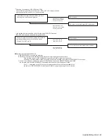
Checking the control signal output from
the MPU/DSP
Points to be checked
Normal voltage
/FRST
D701(Anode side)
1.8V fixed later
D801(Cathode side)
1.8V fixed later
Remove R51 to check the voltage of the SBC.
if the MPU/DSP side is 0V,
the MPU/DSP or Flash Memory or mobile DDR
may be broken.
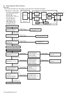
Checking the output signal
from the MPU/DSP.
When a normal
value is confirmed.
When a normal
value is confirmed.
When a normal
value is confirmed.
When a normal
value is confirmed.
When a normal
value is confirmed.
When a normal
value is confirmed.
When an abnormal
value is confirmed.
When an abnormal
value is confirmed.
When an abnormal
value is confirmed.
When an abnormal
value is confirmed.
When an abnormal
value is confirmed.
When an abnormal
value is confirmed.
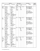
Descriptions of signal names
(1) /RST
:MPU/DSP reset signal
LOW Reset
(2) /BINT
:Battery final voltage monitoring
LOW Final voltage
(3) /OVRB_OUT :Battery overvoltage monitoring
LOW Overvoltage
(4) /PSW_OUT :Power switch signal
LOW ON
(5) /IGN_OUT
:Ignition switch signal
LOW ON
(6) /FRST
:Flash Memory reset signal
LOW Reset
(7) /CS_F
:Flash Memory chip select signal LOW Active
(8) SBC
:B control
HIGH ON
(9) 30LCD
:LCD module control 3.0V power supply
(10) PRST
:LCD reset signal
LOW Reset
(11) /CS_LCD
:LCD controller chip select signal LOW Active
Содержание NX-5700
Страница 106: ...MEMO ...
Страница 137: ...MEMO ...
Страница 138: ... No RA020 Rev 002 VSE Printed in Japan JVC KENWOOD Corporation Communications Systems Business Unit ...

