(No.RA020<Rev.002>)1-21
2.4.6.5
DSP
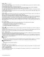
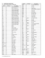
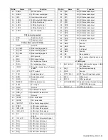
The DSP circuit consists of a MPU/DSP (IC706) and processes the baseband signal. The DSP operates at 288MHz (MAX) clock, the
I/O section operates at 3.3V/1.8V and the core section operates at 1.2V.
The DSP carries out the following processes:
• 4Level FSK processing
• Analog FM pre-emphasis/de-emphasis
• Vocoder processing between audio codec and modulation/demodulation
• CAI processing, such as error correction encoding
• QT/DQT encoding/decoding
• DTMF encoding/decoding
• MSK encoding/decoding
• 2-tone encoding/decoding
• Compressor/expander processing
• Voice scrambler processing
• Transmit/receive audio filtering processing
• Microphone amplifier AGC processing
• Audio mute processing
• Modulation level processing
• Active Noise Reduction
• Voice recording/playback processing
• Voice announce processing
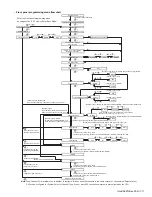
2.4.7 Power Supply Circuit
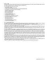
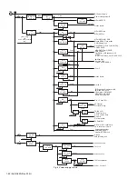
+B voltage is connected to RF Power Module, 50BU regulator (Q8, Q9 and D11) through the fuse (F1), DC/DC converter IC (IC8) via
fuse (F1), SB1 switch (Q5 and Q6) through the fuse (F2) and SB2 switch (Q10 and Q11) through the fuse (F3).
Q8, Q9 and D11 regB voltage to 5V (50BU). Then IC1 regulates 50BU to 3.1V (31BU). Then IC3 regulates 31BU to 1.2V
(12BU). 50BU, 31BU and 12BU operate whB is supplied.
IC8 regB voltage to 5.4V (54M). 54M is controlled by BAT_CNT signal from Power management IC (IC2). When Power switch
is turned on, BAT_CNT signal is controlled by /PSW signal. 54M goes to DC/DC converter (A1, IC11), AVR ICs (IC5, IC4, IC12, IC14,
IC7, IC10, IC6 and IC17).
A1 (12M) is enabled while the 54M is operating. 12M provides the power to the MPU/DSP (IC706) and turns on IC11 (18M). 18M
provides the power to the MPU/DSP and Mobile DDR (IC702) and turns on IC5 (33M), IC14 (33OPT). 33M provides the power to the
MPU/DSP, Flash memory (IC701) and many control circuits and turns on IC4 (33A), IC10 (50A). Then 33A turns on IC9 (18M_3).
The Power management IC (IC2) wB voltage. If +B voltage is higher than 6.2V, IC2 outputs high voltage to the /BINT terminal.
If the /BINT is high, SB1 (Q5 and Q6) and SB2 (Q10 and Q11) are turned on by SBC_2 signal from MPU. In the same way, IC12 (33C)
and IC6 (50C) are turned on by SBC_2. 50C is fed to IC13 (200C). IC13 (200C) is the DC/DC boost converter. The 200C circuit then
outputs approxi20VDC.
SB1 supplies Sub (Display) unit and D-sub 25 with +B voltage. SB2 supplies Audio power amplifier (IC911) and 9V AVR (IC15) with
+B voltage. Then IC15 regB to 9V (90C). Then IC16 regulates 90C to 5V (50CT). If the MPU controls TXC, ANT SW and ASSW
signals to High, Q15, Q16 (90T), Q17, Q18 (90ANT) and Q14 are turned on and transmission circuits are enabled to transmit. If the
MPU controls RXC signal to High, IC17 (50R) is turned on and reception circuits are enabled to receive.
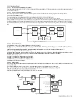
When the Power management IC and MPU detect /PSW signal (Power switch), /IGN signal (Ignition sense) and /BINT signal, they
set the SBC_2 signal to Low, and turn the transceiver power off.
When D1, Q4 detect over-voltage condition, they turn SB1 and SB2 off, and transfer that the MPU through IC2.
Содержание NX-5700
Страница 106: ...MEMO ...
Страница 137: ...MEMO ...
Страница 138: ... No RA020 Rev 002 VSE Printed in Japan JVC KENWOOD Corporation Communications Systems Business Unit ...


