


15 of 43
2020-5-22
UG2020-11 REF-Vacuum-C101-2ED User Guide
however, a high side output transition from low to high when the low side is on can cause switch damage or
unreliable motor operation.
Negative V
S
excursions occur during faster switching events over long PCB traces or wiring harnesses that form
a parasitic inductor. The higher the parasitic inductor value and switching frequency, the larger is the potential
negative V
S
voltage that is developed during a switching event.
Negative V
S
immunity is a key determining factor in selecting a robust gate driver IC that will be more immune
to negative V
S
excursions due to inductive parasitic on the PCB or wiring harness.
In a typical motor drive system, dV/dt is typically designed to be in the range of 3-5 V/ns. The negative transient
voltage can exceed this range during some events such as short-circuit and overcurrent shutdown, when di/dt is
greater than in normal operation.
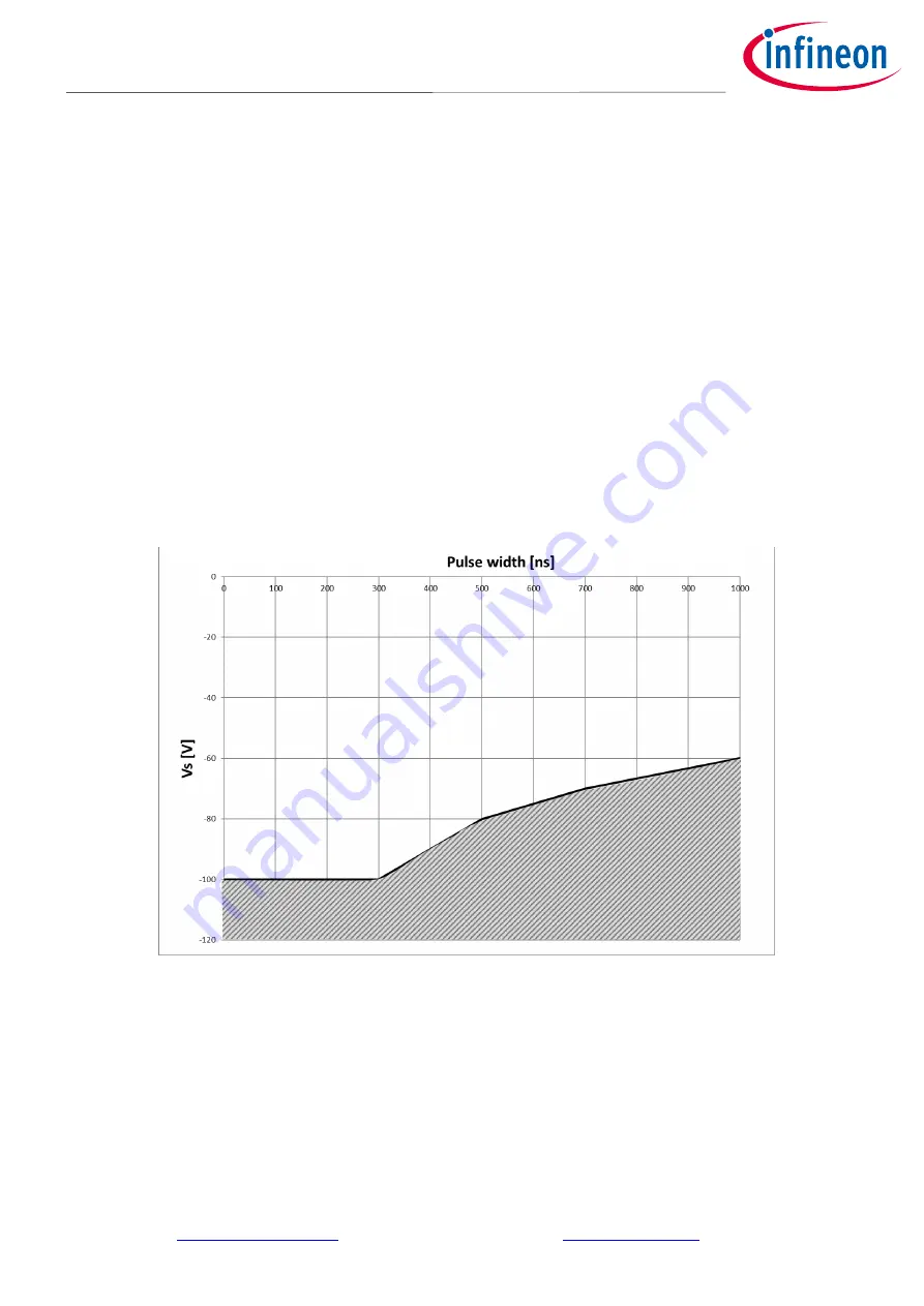
2ED2304S06F has been designed for the robustness required in many of today’s demanding applications. An
indication of the robustness of 2ED2304S06F can be seen in Figure 7, where the 2ED2304S06F safe operating area
(SOA) is shown at V
BS
=15 V based on repetitive negative transient voltage spikes. A negative transient voltage
falling in the gray area (outside SOA) may lead to IC permanent damage; and vice versa, unwanted functional
anomalies or permanent damage to the IC do not appear if negative V
S
transients fall within the SOA.
Figure 7
Negative transient voltage SOA on V
S
pin for 2ED2304S06F @ VBS=15 V
Even though the 2ED2304S06F has been shown to be able to handle these large, negative transient voltage
conditions, it is highly recommended that the circuit designer always limit the negative transient voltage on the
V
S
pin as much as possible by careful PCB layout and component use.


