background image


Embedded Solutions

                          Page  27

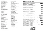
PMC Module Logic Interface Pin Assignment

The figure below gives the pin assignments for the PMC Module PCI Pn2 Interface on
the PMC-Parallel-TTL.   See the User Manual for your carrier board for more
information. Unused pins may be assigned by the specification and not needed by this
design.

+12V

1

2

3

4

GND

5

6

GND

7

8

9

10

11

12

RST#

BUSMODE3#

13

14


BUSMODE4#

15

16

GND

17

18

AD30

AD29

19

20

GND

AD26

21

22

AD24

23

24

IDSEL

AD23

25

26

AD20

27

28

AD18

29

30

AD16

C/BE2#

31

32

GND

33

34

TRDY#

35

36

GND

STOP#

37

38

PERR#

GND

39

40

SERR#

41

42

C/BE1#

GND

43

44

AD14

AD13

45

46

GND

AD10

47

48

AD8

49

50

AD7

51

52

53

54

GND

55

56

57

58

GND

59

60

61

62

GND

63

64

Figure 27

PMC-PARALLEL-TTL Pn2 Interface

Содержание PMC-PARALLEL-TTL

Страница 1: ... DuBois St Suite 3 Santa Cruz Ca 95060 831 457 8891 Fax 831 457 4793 http www dyneng com sales dyneng com Est 1988 User Manual PMC PARALLEL TTL Digital Parallel Interface PMC Module Revision A1 Corresponding Hardware Revision 1 10 2007 0101 FLASH 0101 ...

Страница 2: ... notice Furthermore Dynamic Engineering assumes no liability arising out of the application or use of the device described herein The electronic equipment described herein generates uses and can radiate radio frequency energy Operation of this equipment in a residential area is likely to cause radio interference in which case the user at his own expense will be required to take whatever measures m...

Страница 3: ...eg 18 pmcparttl_COSclk 19 pmcparttl_RisLreg 20 pmcparttl_RisUreg 20 pmcparttl_FallLreg 21 pmcparttl_FallUreg 21 pmcparttl_IntRisLreg 22 pmcparttl_IntRisUreg 22 pmcparttl_IntFallLreg 23 pmcparttl_IntFallUreg 23 pmcparttl_IntRisLstat 24 pmcparttl_IntRisUstat 24 pmcparttl_IntRisLstat 25 pmcparttl_IntRisUstat 25 PMC MODULE LOGIC INTERFACE PIN ASSIGNMENT 26 PMC MODULE LOGIC INTERFACE PIN ASSIGNMENT 27 ...

Страница 4: ...mbedded Solutions Page 4 APPLICATIONS GUIDE 30 Interfacing 30 Construction and Reliability 31 Thermal Considerations 32 Service Policy 33 Out of Warranty Repairs 33 SPECIFICATIONS 34 ORDER INFORMATION 35 ...

Страница 5: ...L TTL COS CLK CONTROL BIT MAP 19 FIGURE 14 PMC PARALLEL TTL RISING LOWER BIT MAP 20 FIGURE 15 PMC PARALLEL TTL RISING UPPER BIT MAP 20 FIGURE 16 PMC PARALLEL TTL FALLING LOWER BIT MAP 21 FIGURE 17 PMC PARALLEL TTL FALLING UPPER BIT MAP 21 FIGURE 18 PMC PARALLEL TTL INT RISING LOWER BIT MAP 22 FIGURE 19 PMC PARALLEL TTL INT RISING UPPER BIT MAP 22 FIGURE 20 PMC PARALLEL TTL INT FALLING LOWER BIT MA...

Страница 6: ...new systems and to upgrade current designs The connector pinouts are retained for ease of system migration The PMC compatible PMC Parallel TTL has 64 independent digital IO The high density makes efficient use of PMC slot resources The IO is available for system connection through the front panel via the rear Pn4 connector or both A high density 68 pin SCSI III front panel connector provides the f...

Страница 7: ...packs also allow for parallel combinations to create more options of specific pull up values For custom models with additional pull ups or alternate values please contact Dynamic Engineering The two columns of pull up resistor locations are visible on the rear of the card Figure 1 PMC PARALLEL TTL REAR VIEW The registers are mapped as 32 bit words and support byte word and 32 bit access All regist...

Страница 8: ...RALLEL TTL is part of the PMC Module family of modular I O components The PMC PARALLEL TTL conforms to the PMC standard This guarantees compatibility with multiple PMC Carrier boards Because the PMC may be mounted on different form factors while maintaining plug and software compatibility system prototyping may be done on one PMC Carrier board with final system implementation on a different one ...

Страница 9: ... allow direct updates if 64 bit synchronization is not required For an IO with the direction bit set and master enabled When a 0 is written to any IO line register position the corresponding line is driven low When a 1 is written to any IO line register position that line is un driven by the local driver and the output level will be controlled by the termination resistor and any other drivers atta...

Страница 10: ... a pulse some time after the address for the IO registers is written to The custom pulse will be more accurate for delay and duration than a SW timing solution The number of accesses to the card can be reduced as well having the effect of greater through put Please contact Dynamic Engineering with your requirements Figure 2 PMC PARALLEL TTL Block Diagram ...

Страница 11: ...er Register define pmcparttl_IntRisLreg 0x003c 15 PMC Parallel TTL Interrupt Enable Rising lower Register define pmcparttl_IntRisUreg 0x0040 16 PMC Parallel TTL Interrupt Enable Rising upper Register define pmcparttl_IntFallLreg 0x0044 17 PMC Parallel TTL Interrupt Enable Falling lower Register define pmcparttl_IntFallUreg 0x0048 18 PMC Parallel TTL Interrupt Enable Falling upper Register define p...

Страница 12: ...ttings can be used except for setting the master output enable and the direction bits corresponding to the channels to transmit on If COS inputs are to be used the reference and divisor clocks may require programming In many cases the default settings will work In addition the Rising Falling and Interrupt capabilities need to be programmed Once the settings are in place it is recommended that the ...

Страница 13: ...pting functions are available as status but no interrupt request is generated by the card to allow for polled operation Force Interrupt when 1 and the master is enabled will cause an interrupt request The interrupt can be cleared by clearing this bit or disabling the master interrupt enable or both Force Interrupt is used for test and software development purposes Master Parallel Data Enable is us...

Страница 14: ...and used to determine which PMC Parallel TTL is which in a system with multiple cards installed The DIPswitch can also be used for other purposes software revision etc The Design ID and Revision are a 16 bit field allowing for 256 designs and 256 revisions of each The base design is 0x01 the current revision is 0x01 As new features are added to the base design the revision will be updated to allow...

Страница 15: ...led bits are active this bit is set The status is captured before the master interrupt enable If the master interrupt enable is set an interrupt will be generated if this condition is true INTR Falling This is the logical OR of the COS outputs for the Falling Edge condition The Falling register will select which bits can be active enabled If any of the enabled bits capture a falling edge this bit ...

Страница 16: ...CRIPTION 31 0 DIR63 32 Figure 8 PMC PARALLEL TTL Direction Upper Bit Map The upper 32 bits of the parallel port direction are controlled with this port When reset this port is cleared 0x00000000 All IO are set to read inputs To use one or more of the IO for outputs program the corresponding direction bit s to 1 Once a Direction bit is set to output the data in the corresponding output holding regi...

Страница 17: ...te datareg port The data read from the data register is a direct read of the state of the IO lines The bits are not modified for level or transition etc Some bits may be defined as outputs The input will match the output definition in this case Local loop back can be performed for the bits where outputs are defined The inputs will match the state of the system when external devices can drive the i...

Страница 18: ...tUreg 20 Data Reg Port read only DATA BIT DESCRIPTION 31 0 Data IO 63 32 Figure 12 PMC PARALLEL TTL Data Reg Upper Bit Map Data written to the Data IO registers can be read back through this port The register is read back instead of the IO side when accessing this port The data will match the state of the data output bits written to the output side of the Data IO register ...

Страница 19: ...ock source The base design oscillator rate is 50 MHz The external clock can be any TTL level source driven onto the External Clock input line The clock should be free running to be used for this purpose POST SELECTOR when 1 sets the output clock to the divided clock when 0 sets the output clock to the pre selector reference value clock source DIVISOR 11 0 are the clock divisor select bits The cloc...

Страница 20: ...er Bit Map The Rising control register bits correspond to the input data bits All IO can be set up for COS activity even if defined as an output In most cases the output bits will be set to 0 for the Rising register When set 1 and the corresponding input bit transitions from low to high the COS register of rising activity will be have the corresponding bit set If the separate interrupt enable bit ...

Страница 21: ...per Bit Map The Falling control register bits correspond to the input data bits All IO can be set up for COS activity even if defined as an output In most cases the output bits will be set to 0 for the Falling register When set 1 and the corresponding input bit transitions from High to Low the COS register of falling activity will be have the corresponding bit set If the separate interrupt enable ...

Страница 22: ...ng Int En 63 32 Figure 19 PMC PARALLEL TTL int Rising Upper Bit Map The Rising Interrupt Enable control register bits correspond to the input data bits All IO can be set up for COS activity even if defined as an output In most cases the output bits will be set to 0 for the Rising Interrupt Enable register When set 1 and the corresponding Rising bit is captured by the COS register an interrupt can ...

Страница 23: ...ing Int En 63 32 Figure 21 PMC PARALLEL TTL int Falling Upper Bit Map The Falling Interrupt Enable control register bits correspond to the input data bits All IO can be set up for COS activity even if defined as an output In most cases the output bits will be set to 0 for the Falling Interrupt Enable register When set 1 and the corresponding falling bit is captured by the COS register an interrupt...

Страница 24: ...COS status upper The COS captured for those bits enabled with the Rising register are held in this register The bits are held until cleared The bits are cleared by writing to the register with the corresponding bit or bits set Writing to the register with the data read will clear the bits the software has read and not clear the bits not set at the time of reading This is the recommended practice t...

Страница 25: ... Falling COS status upper The COS captured for those bits enabled with the Falling register are held in this register The bits are held until cleared The bits are cleared by writing to the register with the corresponding bit or bits set Writing to the register with the data read will clear the bits the software has read and not clear the bits not set at the time of reading This is the recommended ...

Страница 26: ...ification and not needed by this design 12V 1 2 GND INTA 3 4 5 6 BUSMODE1 5V 7 8 9 10 GND 11 12 CLK GND 13 14 GND 15 16 5V 17 18 AD31 19 20 AD28 AD27 21 22 AD25 GND 23 24 GND C BE3 25 26 AD22 AD21 27 28 AD19 5V 29 30 AD17 31 32 FRAME GND 33 34 GND IRDY 35 36 DEVSEL 5V 37 38 GND LOCK 39 40 41 42 PAR GND 43 44 AD15 45 46 AD12 AD11 47 48 AD9 5V 49 50 GND C BE0 51 52 AD6 AD5 53 54 AD4 GND 55 56 AD3 57...

Страница 27: ...assigned by the specification and not needed by this design 12V 1 2 3 4 GND 5 6 GND 7 8 9 10 11 12 RST BUSMODE3 13 14 BUSMODE4 15 16 GND 17 18 AD30 AD29 19 20 GND AD26 21 22 AD24 23 24 IDSEL AD23 25 26 AD20 27 28 AD18 29 30 AD16 C BE2 31 32 GND 33 34 TRDY 35 36 GND STOP 37 38 PERR GND 39 40 SERR 41 42 C BE1 GND 43 44 AD14 AD13 45 46 GND AD10 47 48 AD8 49 50 AD7 51 52 53 54 GND 55 56 57 58 GND 59 6...

Страница 28: ...O_60 5 39 IO_27 IO_59 6 40 IO_26 IO_58 7 41 IO_25 IO_57 8 42 IO_24 IO_56 9 43 IO_23 IO_55 10 44 IO_22 IO_54 11 45 IO_21 IO_53 12 46 IO_20 IO_52 13 47 IO_19 IO_51 14 48 IO_18 IO_50 15 49 IO_17 IO_49 16 50 IO_16 IO_48 17 51 IO_15 IO_47 18 52 IO_14 IO_46 19 53 IO_13 IO_45 20 54 IO_12 IO_44 21 55 IO_11 IO_43 22 56 IO_10 IO_42 23 57 IO_9 IO_41 24 58 IO_8 IO_40 25 59 IO_7 IO_39 26 60 IO_6 IO_38 27 61 IO...

Страница 29: ..._7 7 8 IO_8 IO_9 9 10 IO_10 IO_11 11 12 IO_12 IO_13 13 14 IO_14 IO_15 15 16 IO_16 IO_17 17 18 IO_18 IO_19 19 20 IO_20 IO_21 21 22 IO_22 IO_23 23 24 IO_24 IO_25 25 26 IO_26 IO_27 27 28 IO_28 IO_29 29 30 IO_30 IO_31 31 32 IO_32 IO_33 33 34 IO_34 IO_35 35 36 IO_36 IO_37 37 38 IO_38 IO_39 39 40 IO_40 IO_41 41 42 IO_42 IO_43 43 44 IO_44 IO_45 45 46 IO_46 IO_47 47 48 IO_48 IO_49 49 50 IO_50 IO_51 51 52 ...

Страница 30: ...owered on and part is not It is better to avoid the issue of going past the safe operating areas by powering the equipment together and by having a good ground reference Keep cables short Flat cables even with alternate ground lines are not suitable for long distances The PMC Parallel TTL has transorbs for input protection The connector is pinned out for a standard SCSI II III cable to be used It ...

Страница 31: ...d pins on both plugs and receptacles They are rated at 1 Amp per pin 100 insertion cycles minimum These connectors make consistent correct insertion easy and reliable The PMC is secured against the carrier with the connectors and front panel If more security against vibration is required the stand offs can be secured against the carrier The PMC Module provides a low temperature coefficient of 2 17...

Страница 32: ...l circuitry is very low It is possible to create a higher power dissipation with the externally connected logic If more than one Watt is required to be dissipated due to external loading then forced air cooling is recommended With the one degree differential temperature to the solder side of the board external cooling is easily accomplished ...

Страница 33: ...ny the return Dynamic Engineering will not be responsible for damages due to improper packaging of returned items For service on Dynamic Engineering Products not purchased directly from Dynamic Engineering contact your reseller Products returned to Dynamic Engineering for repair by other than the original customer will be treated as out of warranty Out of Warranty Repairs Out of warranty repairs w...

Страница 34: ...es LW to registers read write to most registers Access Time Frame to TRDY 121 nS 4 PCI clocks Interrupt All IO lines can be used as interrupt sources with programmable rising and or falling activity on IO line COS Onboard Options All Options are Software Programmable Interface Options 68 Pin SCSI III connector at front bezel User IO routed to Pn4 Dimensions Standard Single PMC Module Construction ...

Страница 35: ...O reference Related PCI2PMC PMC to PCI adapter to allow installation of PMC Parallel TTL into a PCI system http www dyneng com pci2pmc html HDEterm68 68 position terminal block with two SCSI II III connectors PMC Parallel TTL compatible http www dyneng com HDEterm68 html HDEcabl68 SCSI II III cable compatible with FPIO on PMC Parallel IO http www dyneng com HDEcabl68 html PIM_Parallel_IO PMC IO Mo...

Отзывы: