Specifications subject to change without notice
© Digital View Ltd – Doc Ver 1.00: 10 Sept, 2021
Page
20 of 46
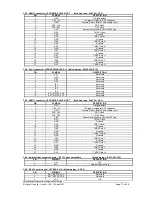
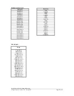
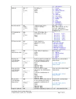
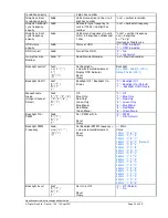
J3 – LVDS output connector: JAE FI-RE51S-HF (Matching type : JAE FI-RE51HL)
PIN
SYMBOL
DESCRIPTION
1
VLCD_HV
Panel power supply (+12V / 18V) (selected by JA3, JA5 & JA6)
2
VLCD_HV
Panel power supply (+12V / 18V) (selected by JA3, JA5 & JA6)
3
VLCD_HV
Panel power supply (+12V / 18V) (selected by JA3, JA5 & JA6)
4
VLCD_HV
Panel power supply (+12V / 18V) (selected by JA3, JA5 & JA6)
5
VLCD_HV
Panel power supply (+12V / 18V) (selected by JA3, JA5 & JA6)
6
VLCD_LV
Panel power supply (3,3V/5V) (selected by JA3, JA5 & JA6)
7
VLCD_LV
Panel power supply (3,3V/5V) (selected by JA3, JA5 & JA6)
8
VLCD_LV
Panel power supply (3,3V/5V) (selected by JA3, JA5 & JA6)
9
VLCD_LV
Panel power supply (3,3V/5V) (selected by JA3, JA5 & JA6)
10
VLCD_LV
Panel power supply (3,3V/5V) (selected by JA3, JA5 & JA6)
11
GND
Ground
12
GND
Ground
13
GND
Ground
14
GND
Ground
15
GND
Ground
16
OP1
-
17
OP2
-
18
OP3
-
19
OP4
-
20
GND
Ground
21
GND
Ground
22
LVDS_
Positive differential LVDS data bit A4
23
LVDS_OUT1_A4-
Negative differential LVDS data bit A4
24
LVDS_
Positive differential LVDS data bit A3
25
LVDS_OUT1_A3-
Negative differential LVDS data bit A3
26
GND
Ground
27
LVDS_
Positive LVDS clock for A channel
28
LVDS_OUT1_AC-
Negative LVDS clock for A channel
29
GND
Ground
30
LVDS_
Positive differential LVDS data bit A2
31
LVDS_OUT1_A2-
Negative differential LVDS data bit A2
32
LVDS_
Positive differential LVDS data bit A1
33
LVDS_OUT1_A1-
Negative differential LVDS data bit A1
34
LVDS_
Positive differential LVDS data bit A0
35
LVDS_OUT1_A0-
Negative differential LVDS data bit A0
36
GND
Ground
37
LVDS_
Positive differential LVDS data bit B4
38
LVDS_OUT1_B4-
Negative differential LVDS data bit B4
39
LVDS_
Positive differential LVDS data bit B3
40
LVDS_OUT1_B3-
Negative differential LVDS data bit B3
41
GND
Ground
42
LVDS_
Positive LVDS clock for B channel
43
LVDS_OUT1_BC-
Negative LVDS clock for B channel
44
GND
Ground
45
LVDS_
Positive differential LVDS data bit B2
46
LVDS_OUT1_B2-
Negative differential LVDS data bit B2
47
LVDS_
Positive differential LVDS data bit B1
48
LVDS_OUT1_B1-
Negative differential LVDS data bit B1
49
LVDS_
Positive differential LVDS data bit B0
50
LVDS_OUT1_B0-
Negative differential LVDS data bit B0
51
GND
Ground
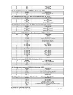
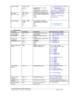
LED1 – Status LED connector: JST B3B-XH-A (Matching type : XHP-3)
PIN
DESCRIPTION
1
Green LED pin (anode)
2
LED pin common (cathode)
3
Red LED pin (anode)
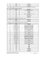
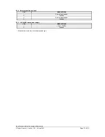
P5 – Connector for firmware upgrade: JST B4B-PH-K compatible (Matching type : PHR-4)
PIN
DESCRIPTION
1
+5V
2
USB Data -
3
USB Data +
4
Ground
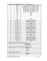
PP2 – Alternate 12V/24VDC input power supply
PIN
DESCRIPTION
1
+12VDC / 24VDC in
2
Ground


