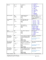
Specifications subject to change without notice
© Digital View Ltd – Doc Ver 1.00: 10 Sept, 2021
Page
19 of 46
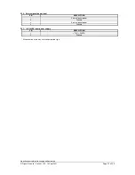
8
-/LEFT
OSD -/Left
9
+/RIGHT
OSD +/Right
10
SEL_DN
OSD Select down
11
SEL_UP
OSD Select up
12
NC
No connection
The VR for brightness depends on the inverter. The main power load for On/Off is handled by a relay on the controller.
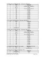
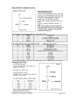
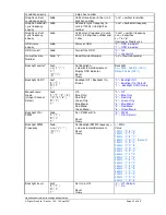
CNV6 - VGA input : HIROSE DF11-12DP-2DSA compatible
PIN
SYMBOL
DESCRIPTION
1
R
Red, analog
2
DDC_5V
+5V power supply for DDC (optional)
3
G
Green, analog
4
GND
Ground
5
B
Blue, analog
6
GND
Ground
7
HS
Horizontal sync or composite sync, input
8
GND
Ground
9
VS
Vertical sync, input
10
DDC_SCL
DDC serial clock
11
NC
No connection
12
DDC_SDA
DDC serial data
IR1 – Infra-Red sensor connector: JST B3B-XH-A (Matching type : XHP-3)
PIN
SYMBOL
DESCRIPTION
1
GND
Ground
2
STDBY_Vcc
Stand by voltage
3
IR Data
IR data
J2 – LVDS output connector: JAE FI-RE41S-HF (Matching type : JAE FI-RE41HL)
PIN
SYMBOL
DESCRIPTION
1
GND
Ground
2
LVDS_OUT2_B0-
Negative differential LVDS data bit B0
3
LVDS_
Positive differential LVDS data bit B0
4
LVDS_OUT2_B1-
Negative differential LVDS data bit B1
5
LVDS_
Positive differential LVDS data bit B1
6
LVDS_OUT2_B2-
Negative differential LVDS data bit B2
7
LVDS_
Positive differential LVDS data bit B2
8
LVDS_OUT2_BC-
Negative LVDS clock for B channel
9
LVDS_
Positive LVDS clock for B channel
10
GND
Ground
11
LVDS_OUT2_B3-
Negative differential LVDS data bit B3
12
LVDS_
Positive differential LVDS data bit B3
13
GND
Ground
14
LVDS_OUT2_B4-
Negative differential LVDS data bit B4
15
LVDS_
Positive differential LVDS data bit B4
16
GND
Ground
17
LVDS_OUT2_A0-
Negative differential LVDS data bit A0
18
LVDS_
Positive differential LVDS data bit A0
19
LVDS_OUT2_A1-
Negative differential LVDS data bit A1
20
LVDS_
Positive differential LVDS data bit A1
21
LVDS_OUT2_A2-
Negative differential LVDS data bit A2
22
LVDS_
Positive differential LVDS data bit A2
23
LVDS_OUT2_AC-
Negative LVDS clock for A channel
24
LVDS_
Positive LVDS clock for A channel
25
GND
Ground
26
LVDS_OUT2_A3-
Negative differential LVDS data bit A3
27
LVDS_
Positive differential LVDS data bit A3
28
GND
Ground
29
LVDS_OUT2_A4-
Negative differential LVDS data bit A4
30
LVDS_
Positive differential LVDS data bit A4
31
GND
Ground
32
GND
Ground
33
GND
Ground
34
GND
Ground
35
GND
Ground
36
GND
Ground
37
NC
No connection
38
NC
No connection
39
NC
No connection
40
NC
No connection
41
NC
No connection


