Physical Description
Table 2–7
Keyboard Connector — AT Style Pin-Out (J39)
Pin
Number
Function
Pin
Number
Function
1
Clock
4
Ground
2
Data
5
+5 V
3
No connection
Table 2–8 lists the pin numbers and functions of the PS/2 keyboard
connector.
Table 2–8
Keyboard Connector — PS/2 Style Pin-Out (J38)
Pin
Number
Function
Pin
Number
Function
1
Data
4
+5 V
2
No connection
5
Clock
3
Ground
6
No connection
2.2.2.9
Keylock and Power LED Connector (J9)
The keylock and power LED (J9) is a 5-position (1 x 5) connector that
serves two purposes:
•
Pins 1 and 3 p5 V and ground for an optional LED indicating
dc power is present.
•
Pins 4 and 5 supply a connection point for a keylock that could be used
for disabling the keyboard.
Table 2–9 lists the pin numbers and functions of the keylock and power
LED connector.
Table 2–9
Keylock and Power LED Connector Pin-Out (J9)
Purpose
Pin Number
Function
Power LED
1
+5 V (through 470 ohm pull-up)
2
No pin installed
3
Ground
Keylock
4
Keylock signal
5
Ground
Figure 2–5 shows the keylock and power LED circuit.
2–10
Содержание AXPpci 33
Страница 10: ......
Страница 14: ......
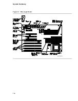
Страница 18: ...System Summary Figure 1 1 Main Logic Board MR 6391 AI 1 4...
Страница 22: ...Physical Description Figure 2 2 MLB Mechanical Drawing MR 6414 AI 2 4...
Страница 23: ...Physical Description Figure 2 3 MLB Component Outline Drawing MR 6401 AI 2 5...
Страница 46: ......
Страница 64: ......
Страница 70: ......
Страница 98: ......


