16
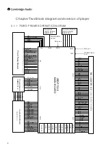
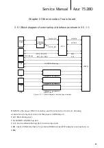
Pt6302
VFD
GRID1~12
SEG1~35
Mt8580
MCU
VDATA
VSTB
VCLK
VFD_OFF
KEY_L/P/U KEY_R_D
OPEN_KEY STBY_KEY
IR_FP_IN
IR_MCU
MCU_ISP_SDA
MCU_ISP_SCL
FL-24V
FLAC1
FLAC2
REST#
VDD
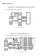
Section VI
Panel and button control circuits
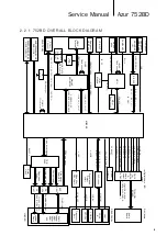
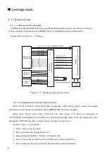
3.6.1: Block diagram of panel circuit:
VFD
power supply
circuit
Reset
circuit
Q1C12
Press
button
Receiver
module
Remote
input and
output circuit
Figure 3.6.1.1 Block diagram of panel
KBP206G
LM 431A
HOST GND
HOST GND
+5V
+15VBD
-15VAU
+15VAU
FB
B1
NCP1271P65
HOST GND
Section 7 Power supply circuit
3.7.1 Block diagram of power supply circuit is shown in figure 3.7.1.1:
Absorbing
circuit
Power system
filter
Power socket
Overvoltage
protection
circuit
Power-off
control
circuit
Switching IC
MOS tube
Tr
an
sf
or
m
er
Opto-
coupler
Rectifying
Rectifying
Rectifying
Rectifying
Rectifying
Filtering
Filtering
Filtering
Filtering
Filtering
Figure 3.7.1.1 Block diagram of power circuit
Sampling
circuit
-14-

