BLUE CHIP ADC-42, Руководство пользователя
Пользовательский мануал для BLUE CHIP ADC-42 доступен для скачивания бесплатно на manualshive.com. Этот руководство поможет вам быстро и легко научиться пользоваться вашим устройством. Не откладывайте, загрузите его прямо сейчас!
Поделиться
Скачать


Отзывы:
Нет отзывов
Похожие инструкции для ADC-42
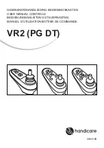
VR2
Бренд: Handicare Страницы: 56

System 10
Бренд: DayTronic Страницы: 414

AL-A 64 kN
Бренд: Habegger Страницы: 2

M4000-PRO
Бренд: Panamax Страницы: 16

CS-AC-4311
Бренд: Controlsoft Страницы: 12

NI 9231
Бренд: National Instruments Страницы: 9

001G4040EZT
Бренд: CAME Страницы: 128

LIP 471R
Бренд: HEIDENHAIN Страницы: 32

6826El
Бренд: Skyjack Страницы: 47

LEADER 25
Бренд: Ebinger Страницы: 48

TC-ME
Бренд: Aiphone Страницы: 2

BBL-4
Бренд: Vestil Страницы: 6

AS-220S
Бренд: golmar Страницы: 44

Agata C200 UK
Бренд: CAME BPT Страницы: 16

PWS BEV-300 Series
Бренд: Pure Water Страницы: 35

Listening System PLS-900
Бренд: Listen Страницы: 2

ADC-1R2
Бренд: SuperLogics Страницы: 24

XVME-500
Бренд: Xycom Страницы: 104


