IPC@CHIP SC2x3
Hardware Manual V1.02 [01.03.09]
©2000-2009 BECK IPC GmbH
Page 26
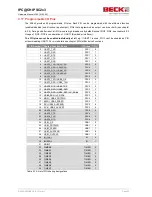
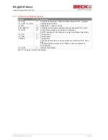
6.1.3 External Local Plus Bus Signals
Signal
I/O
Definition
LP_CS1#,
LP_CS3#.. LP_CS7#
O
Chip Selects (active low), CS[4] and CS[5] shared with ATA, CS[6] and
CS[7] shared with PSC3.
LP_RW
O
Read/Write. 1 = Read, 0 = Write
EXT_AD[31:0]
I/O
AD Address / Data bus (bi-directional when used as data; bit 31=msb)
LP_ACK#
I/O
External Acknowledge input (non-burst transactions),
BURST indication for Most Graphics or Large Flash Modes (Open Drain)
LP_TS#
O
Transfer Start
LP_OE#
O
Output Enable
TSIZ[1:2]
O
Transfer Size
TSIZ bits are available in non-muxed modes on GPIO7 and TEST_SEL_1
pins.
The MUXed Mode provides 3 bits TSIZ[0:2], which are available on
EX_AD[30:28].
LP_ALE#
O
Address Latch Enable
Table 6-1: External Local Plus Bus Signals


