background image

IPC@CHIP SC2x3 

Hardware Manual V1.02 [01.03.09]  


©2000-2009 BECK IPC GmbH 


Page 19


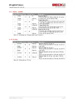
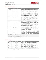
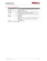
4.14  COP/JTAG-Interface 

Pin Name 

Pin 

Con 

Type 

Description 

JTAG_TCK 

14 

X3 

IN 

JTAG Clock

 (Schmitt Trigger Input with internal 10kOhm 

pullup) 
The (non-reset) behavior of the active TAP and TLM state 
machines is governed by the TMS value at the TCK rising 
edge. TDI value is sampled at the TCK rising edge for all 
shift operations. All TDO non-reset transitions (including 
impedance) occur at the TCK falling edge. All shift register 
capture operations occur at the TCK rising edge. All shift 
register Update operations occur at the TCK falling edge. 

JTAG_TDI 

X3 

IN 

JTAG Data Input

 (with internal 10kOhm pullup) 

Serial test data input can be routed to any IR or DR, as 
determined by the state of the active TAP state machine and 
the contents of the active IR. TDI is sampled at the TCK 
rising edge while the active TAP state machine is in either 
the Shift-IR or Shift-DR state.


JTAG_TDO 

X3 

OUT [8mA] 

JTAG Data Output


TDO when connected to TDI (of another device), TDO 
switches at the TCK falling edge. TDO is driven while the 
TLM state machine is in the Shift-IR or Shift-DR states only; 
it is tri-stated in all other TAP 
states. Except, for the first half clock after exiting the shift 
state, because of its falling edge timing.


JTAG_TMS 

X3 

IN 

JTAG Mode Select

 (with internal 10kOhm pullup) 

TAP state machine control, including TLM. The state of TMS 
at  rising edges of TCK uniquely determines the state 
sequence of the TLM and the active TAP state machines. 
Inactive TAPs ignore TMS completely.


JTAG_TRST# 

11 

X3 

IN 

JTAG Reset

 (Active Low with internal Pull-up) 

When asserted, any on-going JTAG operation is immediately 
aborted.  All  TAP  state  machines,  including  the  TLM, 
immediately  enter  the  Test-Logic-Reset  state.  Other  JTAG 
input  signals  (TCK,  TMS,  and  TDI)  have  no  effect  while 
TRST is asserted. TDO is immediately tri-stated.


TEST_SEL_0 

16 

X3 

IN 


TEST_SEL_1 

12 

X3 

IN 

internal 10kOhm pullup


Table 4-12: Pin Description of COP/JTAG-Interface 


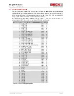
4.15  Interrupts 

Pin Name 

Pin 

Con 

Type 

Description 

IRQ0 

30 

X1 

IN 

Interrupt 0

 (Active High with internal 100kOhm pullup)


This pin is the external interrupt 0 request.


IRQ1 

27 

X1 

IN 

Interrupt 1

 (Active High with internal 100kOhm pullup)


This pin is the external interrupt 0 request.


IRQ2 

28 

X1 

IN 

Interrupt 2

 (Active High with internal 100kOhm pulldown)


This pin is the external interrupt 0 request.


IRQ3 

23 

X1 

IN 

Interrupt 3

 (Active High with internal 100kOhm pulldown)


This pin is the external interrupt 0 request.


Table 4-13: Pin Description of Interrupts 


Содержание IPC@CHIP SC2x3

Страница 1: ...ECK IPC GmbH Page 1 Hardware Manual IPC CHIP Embedded Controller Family SC2x3 MPC5200 High Performance 32 Bit Embedded Processor Computer on Module CoM with Flash RAM Watchdog Order No IPC CHIP Embedd...

Страница 2: ...le is a trademark of Freescale Semiconductor Inc Ethernet is a registered trademark of Xerox Corporation SPI is a trademark of Motorola Inc No part of this guide may be reproduced or transmitted in an...

Страница 3: ...5 1 Mutal Exclusive Functions for USB1 23 5 2 Mutal Exclusive Functions for PSC1 23 5 3 Mutal Exclusive Functions for PSC2 23 5 4 Mutal Exclusive Functions for PSC3 24 5 5 Mutal Exclusive Functions fo...

Страница 4: ...solute Maximum Ratings 35 8 2 Recommended Operating Ranges 35 8 2 1 Voltage and Temperature 35 8 2 2 Supply Current 35 8 2 3 Inputs 36 8 2 4 Outputs 36 8 3 AC Characteristics 37 8 3 1 Muxed Mode 37 8...

Страница 5: ...USB1 UART4 5 Interface 13 Table 4 4 Pin Description of Programmable Serial Controller 1 13 Table 4 5 Pin Description of Programmable Serial Controller 2 14 Table 4 6 Pin Description of Programmable S...

Страница 6: ...me to market The IPC CHIP SC2x3 family of Computer on Modules are embedded processors built on Power Architecture technology and are specially designed for demanding control communication and HMI task...

Страница 7: ...length SRAM 512kByte can be supplied from battery on basis board Parallel Interfaces 10 100 Ethernet MAC ATA IDE Interface Local Plus interface 6 x Programmable Serial Controllers usable as 2 x USB 1...

Страница 8: ...eal Time Clock Chip Selects JTAG SDRA M Mem ory Contr oller XL Bus IP Bus C Bus SDRAM Memory Controller USB two BestComm Intelligent DMA Unit Clock Reset Generation GPIO 16K SRAM IPBI PSC1 PSC2 PSC3 P...

Страница 9: ...IPC CHIP SC2x3 Hardware Manual V1 02 01 03 09 2000 2009 BECK IPC GmbH Page 9 4 Pin Description 4 1 Pin Configuration Figure 4 1 Pin Configuration Looking through Top of Package X3 X1...

Страница 10: ...8 X1 I O 16mA Address Data bus EXT_AD 19 67 X1 I O 16mA Address Data bus EXT_AD 20 64 X1 I O 16mA Address Data bus EXT_AD 21 65 X1 I O 16mA Address Data bus EXT_AD 22 62 X1 I O 16mA Address Data bus E...

Страница 11: ...l pullup LP_OE 96 X1 OUT 8mA Local Plus Bus Output Enable Table 4 1 Pin Description of Local Plus Bus control signals 4 4 ATA Interface Pin Name Pin Con Type Description ATA_IOR 100 X1 OUT 8mA ATA I O...

Страница 12: ...ovides serial Receive Data from the system to serial port 4 4 USB1_RXP 24 X3 IN USB 1 Receive Positive This pin is used to detect single ended zero SEO error conditions and interconnected speed CTS4 I...

Страница 13: ...an be used as PIO0 TXD1 72 X3 OUT RS232 Transmit Data 1 Out This pin provides the signal TXD1 using RS232 level 1 RXD1 PIO1 63 X3 IN I O 4mA Receive Data 1 In This pin provides serial Receive Data fro...

Страница 14: ...as PIO6 2 RTS2 56 X3 OUT 4mA Ready to send 2 Out This pin provides the Ready to Send output for serial port 2 It provides the handshaking output for serial port 2 CAN2TXD OUT 4mA CAN Transmit 2 This...

Страница 15: ...In This pin provides the signal RXD1 using RS232 level 2 RTS3 52 X3 OUT 4mA Ready to send 3 Out This pin provides the Ready to Send output for serial port 3 It provides the handshaking output for seri...

Страница 16: ...rt power output PIO16 I O 4mA This pin can also be used as PIO16 7 MISO 43 X3 IN SPI Master Data In Slave Data Out USB2_SPEED OUT 4mA USB 2 Speed Active High This pin controls the Edge Rate Control 1...

Страница 17: ...Ready to send 6 Out This pin provides the Ready to Send output for serial port 6 It provides the handshaking output for serial port 6 or can be used as PIO23 Table 4 7 Pin Description of Programmable...

Страница 18: ...et Receive Collision Table 4 9 Pin Description of MII 4 12 Timers Pin Name Pin Con Type Description PIO32 32 X3 I O 4mA Internal TIMER0 can only be used as PIO32 TIMER1 PIO33 31 X3 I O 4mA I O 4mA Tim...

Страница 19: ...in all other TAP states Except for the first half clock after exiting the shift state because of its falling edge timing JTAG_TMS 7 X3 IN JTAG Mode Select with internal 10kOhm pullup TAP state machine...

Страница 20: ...VSS GND 50 X3 PWR Power VSS GND 58 X3 PWR Power VSS GND 66 X3 PWR Power VSS GND 74 X3 PWR Power VSS GND 82 X3 PWR Power VSS GND 90 X3 PWR Power VSS GND 98 X3 PWR Power VSS GND 106 X3 PWR Power VSS GND...

Страница 21: ...PC GmbH Page 21 Pin Name Pin Con Type Description GND 74 X1 PWR Power VSS GND 82 X1 PWR Power VSS GND 90 X1 PWR Power VSS GND 98 X1 PWR Power VSS GND 106 X1 PWR Power VSS GND 114 X1 PWR Power VSS GND...

Страница 22: ...XD PSC1 0 1 UART1_RXD PSC1 1 2 UART1_RTS PSC1 2 3 UART1_CTS PSC1 3 4 UART1_DCD PSC1 4 5 UART2_TXD CAN1TXD PSC2 0 6 UART2_RXD CAN1RXD PSC2 1 7 UART2_RTS CAN2TXD PSC2 2 8 UART2_CTS CAN2RXD PSC2 3 9 UART...

Страница 23: ...PRTPWR TXD 7 PIO26 SPEED RTS 8 PIO27 SUSPEND CTS 9 PIO28 OVERCNT PIO28 Table 5 1 Mutal Exclusive Functions for USB1 5 2 Mutal Exclusive Functions for PSC1 Function PSC 1 Nr PIO UART1 UART1e 0 PIO0 TX...

Страница 24: ...MISO MISO MISO SPEED PIO17 MISO 8 PIO18 PIO18 PIO18 SS SS SS SUSPEND PIO18 SS 9 PIO19 PIO19 PIO19 CLK CLK CLK OVRCNT PIO19 CLK Table 5 4 Mutal Exclusive Functions for PSC3 5 5 Mutal Exclusive Function...

Страница 25: ...Selects 2 Chip Select CS signals Programmable Wait States per CS Programmable Deadcycles per CS Programmable Byte Swapping per CS Dynamic bus sizing on some interfaces Support of BURST MODE FLASH devi...

Страница 26: ...1 0 I O AD Address Data bus bi directional when used as data bit 31 msb LP_ACK I O External Acknowledge input non burst transactions BURST indication for Most Graphics or Large Flash Modes Open Drain...

Страница 27: ...AD 24 D8 D0 A24 D0 D8 D24 EXT_AD 23 D7 A23 A23 0 D7 D23 EXT_AD 22 D6 A22 A22 0 D6 D22 EXT_AD 21 D5 A21 A21 0 D5 D21 EXT_AD 20 D4 A20 A20 0 D4 D20 EXT_AD 19 D3 A19 A19 0 D3 D19 EXT_AD 18 D2 A18 A18 0 D...

Страница 28: ...sfer using several industry standard communications protocols The asynchronous serial ports support the following features Full duplex operation 512 byte FIFO 7 bit or 8 bit data transfers Odd even ma...

Страница 29: ...only be repaired by programming it through the serial bootloader interface on UART1 For this reason the pre installed bootloader observes UART1_TXD and UART1_RXD to recognize a RTOS update via the pro...

Страница 30: ...eceiver In addition devices can also be configured as masters or slaves A master is the device that initiates a data transfer on the bus and generates the clock signals to permit that transfer Any oth...

Страница 31: ...put output I O port that allows a serial bit stream of programmed length one to eight bits to be shifted into and out of the device at a programmable bit transfer rate SPI is an industry standard comm...

Страница 32: ...table shows the most common possible baud rates For more information to provided baud rates see RTOS API documentation 50 KBit s 125 KBit s 250 KBit s 500 KBit s 1 MBit s Table 6 3 Provided CAN baud r...

Страница 33: ...f the module has the following functions Monitoring the voltage used on the module 3 3V 1 8V 1 5V External Reset Input Battery back up function for SRAM Battery supply not on the module Chip Select Ga...

Страница 34: ...g edge 25 PSC3_9 PIO19 any transition pulse rising edge falling edge 26 PSC6_0 PIO20 any transition pulse rising edge falling edge 27 PSC6_1 PIO21 any transition pulse rising edge falling edge 28 USB1...

Страница 35: ...VCC 0 3 V Table 8 1 Absolute Maximum Ratings 8 2 Recommended Operating Ranges 8 2 1 Voltage and Temperature Under operating ranges unless otherwise noted Note Exposure to conditions beyond those list...

Страница 36: ...8 4 Inputs 8 2 4 Outputs Parameter Min Typ Max Unit VOL Output Voltage Low IOL max 0 4 V VOH Output Voltage High IOH max 2 4 V Low level output current VOL 0 4V 4mA 4 mA Low level output current VOL...

Страница 37: ...dware Manual V1 02 01 03 09 2000 2009 BECK IPC GmbH Page 37 8 3 AC Characteristics 8 3 1 Muxed Mode Figure 8 1 Timing Diagram MUXed Mode Rastereinstellungen Abstand horizontal 0 15 Abstand vertikal 0...

Страница 38: ...IPC CHIP SC2x3 Hardware Manual V1 02 01 03 09 2000 2009 BECK IPC GmbH Page 38 Figure 8 2 Timing Diagram MUXed Mode 8 3 2 Non Muxed Mode...

Страница 39: ...IPC CHIP SC2x3 Hardware Manual V1 02 01 03 09 2000 2009 BECK IPC GmbH Page 39 Figure 8 3 Timing Diagram Non MUXed Mode...

Страница 40: ...kage Information 9 1 Dimensions Figure 9 1 Package Dimensions Top view through the conductor board 9 2 SC2x3 Connector Board to Board connection via a 120 pole connector with 0 8 mm spacing Manufactur...

Страница 41: ...o program images to the SC2x3 Chiptool can be started and configured through command line parameters This can be used to remote chiptool from other applications to program SC2x3 in series with high qu...

Страница 42: ...ions appearing in BECK IPC GmbH Terms and Conditions of Sale only BECK IPC GmbH MAKES NO WARRANTY EXPRESS STATUTORY IMPLIED OR BY DESCRIPTION REGARDING THE INFORMATION SET FORTH HEREIN OR REGARDING TH...

Отзывы: