Copyright © 2003 Avnet, Inc. AVNET and the AV logo are registered trademarks of Avnet, Inc. All other trademarks are property of their respective owners.
Avnet Electronics Marketing
6 of 33
Rev 1.0 04/17/2006
Released
Literature # ADS-005104
Spartan 3
XC3S2000-FG676
RS232
Clocks:
Socket
66MHz
100MHz
125MHz diff. (opt.)
Switches
Dip(8)
P.B.(2)
181 I/O
AVBus
16MB Flash /
2MB SRAM
Configuration
LEDs
(8)
128x64 OLED
Display
63 I/O
32
50-Pin Header
4 I/O
47 I/O
P4 JTAG
Fly-wire
Header
10/100
Ethernet PHY
USB2.0
Cypress FX2
19 I/O
Platform Flash
XCFxxP
(08-32)
or
(2) XCF04S
32MB DDR SDRAM
(1500 & 2000 only)
63 I/O
16
13 I/O
2x16 Char. LCD
Bus Switches
Audio
Codec
UBC1400
RGB DAC
ADV7123
29
7
AVBus
PS2
PS2
Buzzer
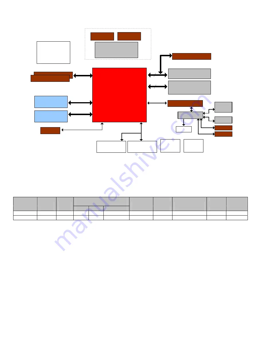
Figure 4 - Spartan-3 Development Board Block Diagram
2.1 Spartan-3
FPGA
The Spartan-3 Development board was designed to support the Spartan-3 FPGA in the 676-pin, BGA package (FG676). The FG676
package supports three mid-range densities (1000, 1500, and 2000). The board was designed to support two of the three densities: the
3S1500 and 3S2000. The schematic symbol used for the Spartan-3 device indicates the specific I/O pins available in each density (396
I/Os with 2VP7 and 556 I/Os with the 2VP20/30). Table 3 describes the attributes of the Spartan-3 device based on density.
Spartan-3
System
Logic
CLB Array
(One CLB=Four Slices)
BlockRAM
Dedicated
Max
Part
Gates
Cells
Rows
Col
Total CLBs
(bits)
BRAM
Multipliers
DCMs
User I/O
XC3S1500 1.5M 29,952 64 52 3,328
576K
32
32
4
XC3S2000 2M 46,080 80 64
5,120
720K
40
40
4
Table 2 - Spartan-3 Attributes by Density
2.2 Configuration
The Spartan-3 Development board supports Boundary-scan as well as Master/Slave Serial and Master/Slave Parallel(SelectMAP)
using the on-board PROMs. All configuration pins are brought out to “J1”, should the user wish to program with an alternate method.
2.2.1 Boundary
scan
Programming the Spartan-3 FPGA via Boundary-scan requires a JTAG download cable (not included in the kit). The Spartan-
3 Development board has connectors to support both the flying leads connection of the Parallel Cable III and the ribbon cable
connection of the Parallel Cable IV. These connectors are labeled “J1” and “J5” respectively.
The FPGA and Platform Flash are both in the JTAG chain and both may be configured via the chain. When programming the
FPGA via the JTAG interface, it is good practice to place the device in Boundary Scan mode. This may be accomplished
using the Mode select jumpers at JP2. The jumper positions are labeled M0 – M2 and are all LOW by default. So placing a
jumper provides a HIGH. The Spartan-3 FPGA is set to Master Serial mode when no jumpers are installed on JP2. To set the
FPGA to boundary-scan mode, install shunts on JP2 at locations 1-2 & 5-6 as shown in below. Note that power should be
removed when changing Mode select jumpers.


