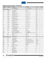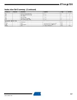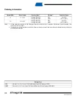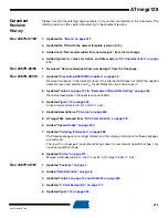
364
2467S–AVR–07/09
ATmega128
Notes:
1. For compatibility with future devices, reserved bits should be written to zero if accessed. Reserved I/O memory addresses
should never be written.
2. Some of the status flags are cleared by writing a logical one to them. Note that the CBI and SBI instructions will operate on
all bits in the I/O register, writing a one back into any flag read as set, thus clearing the flag. The CBI and SBI instructions
work with registers $00 to $1F only.
$01 ($21)
PINE
PINE7
PINE6
PINE5
PINE4
PINE3
PINE2
PINE1
PINE0
$00 ($20)
PINF
PINF7
PINF6
PINF5
PINF4
PINF3
PINF2
PINF1
PINF0
Register Summary (Continued)
Address
Name
Bit 7
Bit 6
Bit 5
Bit 4
Bit 3
Bit 2
Bit 1
Bit 0
Page
Содержание ATmega128
Страница 384: ...vi 2467S AVR 07 09 ATmega128 Rev 2467C 02 02 377 Table of Contents i...
Страница 385: ...vii 2467S AVR 07 09 ATmega128...

