232
2467S–AVR–07/09
ATmega128
Operation
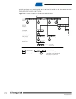
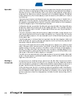
The ADC converts an analog input voltage to a 10-bit digital value through successive approxi-
mation. The minimum value represents GND and the maximum value represents the voltage on
the AREF pin minus 1 LSB. Optionally, AVCC or an internal 2.56V reference voltage may be
connected to the AREF pin by writing to the REFSn bits in the ADMUX Register. The internal
voltage reference may thus be decoupled by an external capacitor at the AREF pin to improve
noise immunity.
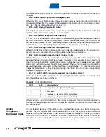
The analog input channel and differential gain are selected by writing to the MUX bits in
ADMUX. Any of the ADC input pins, as well as GND and a fixed bandgap voltage reference, can
be selected as single ended inputs to the ADC. A selection of ADC input pins can be selected as
positive and negative inputs to the differential gain amplifier.
If differential channels are selected, the differential gain stage amplifies the voltage difference
between the selected input channel pair by the selected gain factor. This amplified value then
becomes the analog input to the ADC. If single ended channels are used, the gain amplifier is
bypassed altogether.
The ADC is enabled by setting the ADC Enable bit, ADEN in ADCSRA. Voltage reference and
input channel selections will not go into effect until ADEN is set. The ADC does not consume
power when ADEN is cleared, so it is recommended to switch off the ADC before entering power
saving sleep modes.
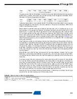
The ADC generates a 10-bit result which is presented in the ADC Data Registers, ADCH and
ADCL. By default, the result is presented right adjusted, but can optionally be presented left
adjusted by setting the ADLAR bit in ADMUX.
If the result is left adjusted and no more than 8-bit precision is required, it is sufficient to read
ADCH. Otherwise, ADCL must be read first, then ADCH, to ensure that the content of the data
registers belongs to the same conversion. Once ADCL is read, ADC access to data registers is
blocked. This means that if ADCL has been read, and a conversion completes before ADCH is
read, neither register is updated and the result from the conversion is lost. When ADCH is read,
ADC access to the ADCH and ADCL Registers is re-enabled.
The ADC has its own interrupt which can be triggered when a conversion completes. When ADC
access to the data registers is prohibited between reading of ADCH and ADCL, the interrupt will
trigger even if the result is lost.
Starting a
Conversion
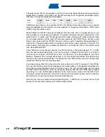
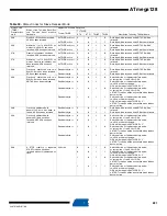
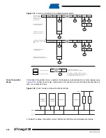
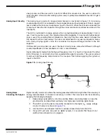
A single conversion is started by writing a logical one to the ADC Start Conversion bit, ADSC.
This bit stays high as long as the conversion is in progress and will be cleared by hardware
when the conversion is completed. If a different data channel is selected while a conversion is in
progress, the ADC will finish the current conversion before performing the channel change.
In Free Running mode, the ADC is constantly sampling and updating the ADC Data Register.
Free Running mode is selected by writing the ADFR bit in ADCSRA to one. The first conversion
must be started by writing a logical one to the ADSC bit in ADCSRA. In this mode the ADC will
perform successive conversions independently of whether the ADC Interrupt Flag, ADIF is
cleared or not.
Содержание ATmega128
Страница 384: ...vi 2467S AVR 07 09 ATmega128 Rev 2467C 02 02 377 Table of Contents i...
Страница 385: ...vii 2467S AVR 07 09 ATmega128...

