89
2467S–AVR–07/09
ATmega128
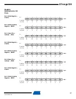
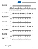
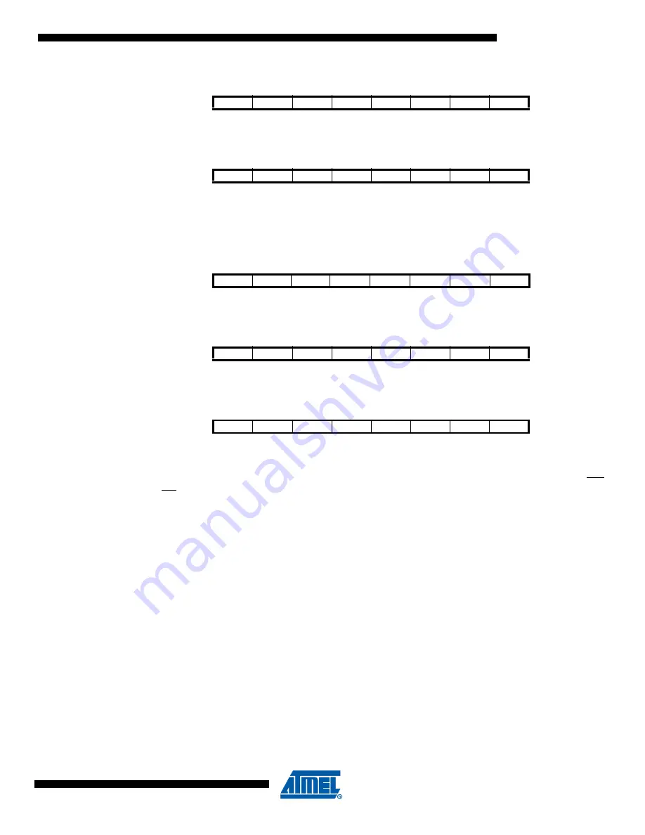
Port F Data Direction
Register – DDRF
Port F Input Pins
Address – PINF
Note that PORTF and DDRF Registers are not available in ATmega103 compatibility mode
where Port F serves as digital input only.
Port G Data Register –
PORTG
Port G Data Direction
Register – DDRG
Port G Input Pins
Address – PING
Note that PORTG, DDRG, and PING are not available in ATmega103 compatibility mode. In the
ATmega103 compatibility mode Port G serves its alternate functions only (TOSC1, TOSC2, WR,
RD and ALE).
Bit
7
6
5
4
3
2
1
0
DDF7
DDF6
DDF5
DDF4
DDF3
DDF2
DDF1
DDF0
DDRF
Read/Write
R/W
R/W
R/W
R/W
R/W
R/W
R/W
R/W
Initial Value
0
0
0
0
0
0
0
0
Bit
7
6
5
4
3
2
1
0
PINF7
PINF6
PINF5
PINF4
PINF3
PINF2
PINF1
PINF0
PINF
Read/Write
R
R
R
R
R
R
R
R
Initial Value
N/A
N/A
N/A
N/A
N/A
N/A
N/A
N/A
Bit
7
6
5
4
3
2
1
0
–
–
–
PORTG4
PORTG3
PORTG2
PORTG1
PORTG0
PORTG
Read/Write
R
R
R
R/W
R/W
R/W
R/W
R/W
Initial Value
0
0
0
0
0
0
0
0
Bit
7
6
5
4
3
2
1
0
–
–
–
DDG4
DDG3
DDG2
DDG1
DDG0
DDRG
Read/Write
R
R
R
R/W
R/W
R/W
R/W
R/W
Initial Value
0
0
0
0
0
0
0
0
Bit
7
6
5
4
3
2
1
0
–
–
–
PING4
PING3
PING2
PING1
PING0
PING
Read/Write
R
R
R
R
R
R
R
R
Initial Value
0
0
0
N/A
N/A
N/A
N/A
N/A
Содержание ATmega128
Страница 384: ...vi 2467S AVR 07 09 ATmega128 Rev 2467C 02 02 377 Table of Contents i...
Страница 385: ...vii 2467S AVR 07 09 ATmega128...


