


the reference and resistor R113 programs the reference to zero if the front panel is disconnected.
Components C43 and R115 provide the current loop frequency compensation. Diodes D42 and D43
keep U7/B in its “active” region when the current loop is not regulating to allow fast transfer to cur-
rent limiting when required.
Voltage error amplifier U8/A works in a similar manner to the current error amplifier sensing the out-
put voltage from U8/B, with voltage reference through R116, R117 and C61, with compensation
R81, R118, C48, C49 and clamping with Diode D45, D46.
Diodes D36, D41 and D44 “OR” the outputs of the error amplifiers so that any one of the amplifiers
can reduce the output of the rectifier by it’s output going in a positive direction. Transistor Q24 is a
current mirror used to level translate the control signal to the -12 volt common of the pulse width
modulator IC U6 with the help of resistors R66 and R77. Transistor Q31 buffers the control signal to
pin 1 of PWM IC U6. Transistor Q23 keeps U8/A in the “active” region to prevent excessive control
delay when the output of the rectifier is suddenly OFF loaded.
Transistor Q33 reduces the output current of the rectifier at excessive heatsink temperatures which
might occur if the cooling air flow is blocked. Negative temperature coefficient resistor R98 mounted
on the rectifier heatsink starts Q33 to conduct at heatsink temperatures in excess of 90 deg. C, thus
reducing the current reference voltage at the input of U7/B.
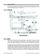
7.1.7
Pulse Width Modulator
The pulse width modulator circuitry consists of current mode control integrated circuit U6, quad
comparator U5 and associated components. IC U6 provides a +5.0 volt (wrt-12V) reference at pin 8
(TP6 wrt TP5), bypassed by C45 and is used in its timing and ramp generator circuitry.
The circuit consisting of comparator U5/A, Transistor Q4, capacitor C19 and current mirror transistor
Q5 is the unit’s oscillator and timing ramp generator. Resistor R31 and diode D8 form a current sink
which charges precision capacitor C19 creating a negative going ramp voltage across C19. Transis-
tor Q5 with resistor R23 form a current mirror which causes a positive going ramp voltage to exist
across R33. When the voltage across R32 exceeds approximately 1 volt as determined by resistor
divider R25, R14 and R33 the output of comparator U5/A goes suddenly low which causes transis-
tor Q4 to discharge C19, terminating the ramp.
Comparator U5/D compares the ramp across R32 to a fixed voltage across R33. When the voltage
across R32 exceeds this level the output of 5/D goes negative determining the maximum conduc-
tion time of the main transistor switch. This output is processed through R19, 21 and R76 and tran-
sistor Q2 to provide the clock and “dead” time input to U6 at pin 4. The negative transition of the
voltage at pin 4 through C18 causes Q3 to transmit a pulse through T5 to turn off the auxiliary
switch Q19 prior to turn ON of the main switch. Pin 6 of U6 goes high approximately 300 ns after
pin 4 goes low, to turn on this main switch via C36, Q22 and T4 provided that the control voltage at
pin 1 is above approximately 1.4 volts, IC U6 monitors the current through the main switch via cur-
rent transformer T8, diodes D34, D39, resistors R61, R62 and 72. Transistor Q6 acts as a current
source similar to Q5 to add a ramp onto the current sense voltage pin 3 of U6 to prevent any cycle
by cycle instabilities at large duty cycles. When the main switch current reaches a level dependent
upon the control voltage at pin 1 U6, the drive output pin 6 goes low and the main switch is turned
off by a pulse through T3 via Q21 and C16.
Transistor Q25 keeps the converter off by reducing the control voltage at Pin 1 of U6 to below 1.4
volts unless the ON/OFF input from the front panel circuitry is held low. Capacitor C44 and resistor
R70 provides a 3 second soft start at turn on. Transistor Q7 disables the clock with the ON/OFF in-
put high to assure a positive rectifier turn off if any component of the power circuitry is faulty.
Document #010-002-C0 Rev. H Page 24
ARGUS TECHNOLOGIES
Содержание RST 48/30
Страница 1: ...RST 48 30 Switched Mode Rectifier Eliminator 010 006 B0 ...
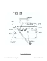
Страница 24: ...Document 010 002 C0 Rev H Page 14 ARGUS TECHNOLOGIES Figure 3 Front Panel Layout ...
Страница 52: ......
Страница 53: ......
Страница 63: ......
Страница 75: ......