


using a shunt resistor and scaling amplifier to compare the output current to the desired maximum
output current to provide a current error signal.
These signals are fed into the pulse width modulator (PWM) via an OR Gate so that either voltage
or current regulation is achieved. The pulse width modulator controls the “ON” time of the switching
transistors to vary the output as commanded by the error amplifiers. It also senses the switching
transistor current on an instantaneous basis to provide cycle by cycle protection of the switching
transistors. An auxiliary supply powered via a small 50/60 Hz transformer powers the control circuit
and front panel circuitry. The PWM receives an ON/OFF command and clock signal from the front
panel circuit.
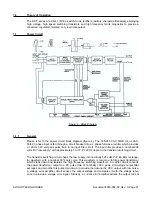
(Please refer to chassis schematic and power PCB schematic)
7.1.2
Input Circuit
The power input cables connect directly to the input side of CB1. Capacitors C1, C2 , C3, C84,
C85, and C86 form part of the input electromagnetic inference (EMI) filter. Resistors R1 and R2 are
used to discharge C84-86 for safety reasons. On first application of power, contactor K1 is open al-
lowing the filter capacitor charging current to be limited by the chassis mounted resistor R6 and R7
Contactor K1 is closed via a command from the front panel circuit. Contacts 5-8 of K1 provide inter-
lock information to the front panel circuitry to prevent operation of the converter circuit unless K1 is
closed.
Iron core inductor L1 forms a subcritical inductor-capacitor filter along with storage capacitor C4 to
provide high power factor and low TIF. Heatsink mounted, full wave bridge diode assemblies D1
and D2 rectifies the input waveform. The storage capacitors stores energy during the ebbs of the
rectifier input waveform to power the transistor circuit. Transient absorbing zener diodes D61 and
D62 provide transient protection. Resistors R4 and R5 provide a current source for a +12 volt
(TP26, with respect to, TP25) primary side auxiliary supply across D5 and also bleed the energy off
C4 at power down.
Inductors L2 and L3 provide common and differential EMI filtering respectively with C1-C3, C22,
C84-C86 respectively. Capacitors C10 and C11 provide a low impedance output for the raw supply
and a path for the high frequency switching current. Capacitor C12 and chassis mounted resistor
R8 provide a damper for the low frequency and high frequency (EMI) input filters and allow the rec-
tifier to operate from an inductive (generator) source.
7.1.3
Transistor Switching Circuit
The converter is a modified form of the forward converter employing one main switch (paralleled
transistors Q9, Q10, Q11) and a demagnetizing switch Q19. Transistors Q9, Q10 and 11 are emit-
ter driven by MOSFET transistors Q12, Q13 and Q14. A current transformer T6 provides base drive
current for Q9, Q10 and Q11 via diode D18. Diode D11 is part of a baker clamp along with the ex-
tension of the secondary of T6 which prevents deep saturation of Q9, 10 and 11 to allow minimal
storage time. A clamp consisting of diode D19 and zener diode D20 protects D18 from excessive
reverse voltages. MOSFET transistor Q8 is used to initiate conduction of the transistor switch at low
loads.
A gate-driving circuit consisting of transistor Q16, diode D22 and capacitor C27 is driven by turn on
pulse transformer T4 and turn off pulse transformer T3. This circuit provides a fast rise and fall time
drive for the emitter drive MOSFETS. Diode D12 and resistor R42 provide clamping of the gate volt-
age. Resistor R9 and R10 are is used to initiate conduction of the transistor switches for low output
current conditions. When the emitters of Q9, (10) and 11 are open circuited by Q12, (13) and 14,
the collector emitter current is diverted out of the bases into capacitors C24 and C25. This rapidly
Document #010-002-C0 Rev. H Page 22
ARGUS TECHNOLOGIES
Содержание RST 48/30
Страница 1: ...RST 48 30 Switched Mode Rectifier Eliminator 010 006 B0 ...
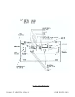
Страница 24: ...Document 010 002 C0 Rev H Page 14 ARGUS TECHNOLOGIES Figure 3 Front Panel Layout ...
Страница 52: ......
Страница 53: ......
Страница 63: ......
Страница 75: ......


