background image

AXM-

A75 User’s Manual


Multifunction I/O Mezzanine Board 


_____________________________________________________________________________________ 

- 28 - 

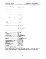
Gain Error (all gains)

3

 .................... 0.01

 typical, 0.1

 maximum 

Gain vs. Temperature .................... 3 ppm/°C typical 

10 pm/°C maximum 

Difference Amplifier 

Device ............................................ TI INA159 
Gain Error ...................................... ±0.005% typical 

±0.024% maximum 

Gain Error vs. Temperature .......... ±1 ppm/°C typical 
Offset Error ................................... ±100 µV typical 

±500 µV maximum 

Offset Voltage vs. Temperature .... ±1.5 µV/°C typical  
Reference Divider Accuracy .......... ±0.002% typical 

±0.024% maximum 

Voltage Reference REF3240 

Device ............................................ TI REF3240 
Accuracy ........................................ 0.01% typical 

±0.2% maximum 

Output Voltage Temperature Drift 4 ppm/°C typical 

7 ppm/°C maximum 

Thermal Hysteresis

4

 ...................... 100 ppm first cycle 

25 ppm additional cycles 

Noise ............................................. 78 µV RMS typical 

Analog to Digital Converter 

ADC ................................................ ADI AD7686 
A/D Resolution .............................. 16-bits 
Data Format .................................. straight binary  
No Missing Codes .......................... no missing codes 15-bits 
A/D Integral Linearity Error ........... 

0.6 LSB typical 

2 LSB maximum 

Offset Error ................................... 

0.1 mV typical 

10 V range 

1.6 mV maximum 

Gain Error Temperature Drift ....... 

0.3 ppm/°C typical 

Offset Temperature Drift .............. 

0.3 ppm/°C typical 

Full Scale Error .............................. 

0.5

 maximum 

A/D Conversion Time .................... 2 

S maximum 

Conversion Rate ............................ 500 kHz maximum 
Input Noise .................................... 2 LSB rms typical 
                                                           

3

 Software calibration eliminates these error components 

4

 Acromag does not temperature cycle this product before shipping to customers.  If the product is operated at the 

extremes of its temperature range, the voltage reference could drift by the amount specified for first cycle.   

Содержание AXM-A75

Страница 1: ...l service in house repair center WE BUY USED EQUIPMENT Sell your excess underutilized and idle used equipment We also offer credit for buy backs and trade ins www artisantg com WeBuyEquipment REMOTE INSPECTION Remotely inspect equipment before purchasing with our interactive website at www instraview com LOOKING FOR MORE INFORMATION Visit us on the web at www artisantg com for more information on ...

Страница 2: ...USER S MANUAL ACROMAG INCORPORATED 30765 South Wixom Road Wixom MI 48393 2417 U S A Tel 248 295 0310 Email solutions acromag com Copyright 2013 Acromag Inc Printed in the USA Data and specifications are subject to change without notice 8500927G ...

Страница 3: ...eset Register Read Write PCIBar2 8000H 14 Control Register Read Write PCIBar2 8100H 15 Status Register 0 Read Write PCIBar2 8104H 16 Status Register 1 Read Write PCIBar2 8108H 16 Digital I O Read Write PCIBar2 810CH 16 Conversion Timer Register Read Write PCIBar2 8110H 16 FLASH Data Register Read Write PCIBar2 8114H 17 Digital I O Direction Register Read Write PCIBar2 8118H 17 ADC Channels 17 ADC ...

Страница 4: ...ERVICE PROCEDURE 25 WHERE TO GET HELP 25 6 0 SPECIFICATIONS 26 Physical 26 Connectors 26 Environmental 26 Power Requirements 27 ANALOG INPUTS 27 Programmable Gain Instrumentation Amplifier 27 Difference Amplifier 28 Voltage Reference REF3240 28 Analog to Digital Converter 28 ANALOG OUTPUTS 29 Digital to Analog Converter 29 7 0 APPENDIX 30 CABLE MODEL 5028 420 Ultra SCSI VHDCI male to SCSI 3 male R...

Страница 5: ... is very important for the user to consider the possible adverse effects of power wiring component sensor or software failures in designing any type of control or monitoring system This is especially important where economic property loss or human life is involved It is important that the user employ satisfactory overall system design It is agreed between the Buyer and Acromag that this is the Buy...

Страница 6: ...AC channels provide simultaneous update with a maximum rate of 100 KHz Programmable Output Voltage Range three gain selections are available that allow a bipolar output voltage range from 10 Volts to 10 5263 Volts Calibration Constants factory calibration constants used to correct gain and offset errors are stored in on board FLASH memory Correction constants are stored for each channel and gain s...

Страница 7: ...N FOR USE UNPACKING AND INSPECTION Upon receipt of this product inspect the shipping carton for evidence of mishandling during transit If the shipping carton is badly damaged or water stained request that the carrier s agent be present when the carton is opened If the carrier s agent is absent when the carton is opened and the contents of the carton are damaged keep the carton and packing material...

Страница 8: ...or some concern Most if not all computer chassis do not provide a fan for cooling of add in boards The dense packing of the mezzanine modules to the carrier board alone results in elevated module and carrier board temperatures and the restricted air flow within the chassis aggravates this problem Adequate air circulation must be provided to prevent a temperature rise above the maximum operating te...

Страница 9: ...7 5 GND 39 DIO8 6 DIO9 40 DIO10 7 DIO11 41 DIO12 8 DIO13 42 DIO14 9 DIO15 43 GND 10 VOUT1 44 GND 11 VOUT2 45 GND 12 VOUT3 46 GND 13 VOUT4 47 GND 14 VOUT5 48 GND 15 VOUT6 49 GND 16 VOUT7 50 GND 17 VOUT8 51 GND 18 GND 52 VIN16 19 VIN16 53 VIN15 20 VIN15 54 VIN14 21 VIN14 55 VIN13 22 VIN13 56 VIN12 23 VIN12 57 VIN11 24 VIN11 58 VIN10 25 VIN10 59 VIN9 26 VIN9 60 VIN8 27 VIN8 61 VIN7 28 VIN7 62 VIN6 29...

Страница 10: ... by multiple ground connections 3 0 PROGRAMMING INFORMATION This Section provides the specific information necessary to program and operate the mezzanine board This mezzanine board is intended only for use on specific Acromag PMC XMC FPGA modules As such only a small portion of I O memory space is currently reserved for operation of the mezzanine board The remaining memory space is defined in the ...

Страница 11: ...4 821B ADC 2 offset 8218 821F unused 821C 8223 ADC 3 data 8220 8227 ADC 3 gain correction 8224 822B ADC 3 offset 8228 822F unused 822C 8233 ADC 4 data 8230 8237 ADC 4 gain correction 8234 823B ADC 4 offset 8238 823F unused 823C 8243 ADC 5 data 8240 8247 ADC 5 gain correction 8244 824B ADC 5 offset 8248 824F unused 824C 8253 ADC 6 data 8250 8257 ADC 6 gain correction 8254 825B ADC 6 offset 8258 825...

Страница 12: ...unused 82BC 82C3 ADC 13 data 82C0 82C7 ADC 13 gain correction 82C4 82CB ADC 13 offset 82C8 82CF unused 82CC 82D3 ADC 14 data 82D0 82D7 ADC 14 gain correction 82D4 82DB ADC 14 offset 82D8 82DF unused 82DC 82E3 ADC 15 data 82E0 82E7 ADC 15 gain correction 82E4 82EB ADC 15 offset 82E8 82EF unused 82EC 82F3 ADC 16 data 82F0 82F7 ADC 16 gain correction 82F4 82FB ADC 16 offset 82F8 82FF unused 82FC 8303...

Страница 13: ... 4 fine gain 8338 833F DAC 4 offset 833C 8343 DAC 5 data 8340 8347 DAC 5 coarse gain 8344 834B DAC 5 fine gain 8348 834F DAC 5 offset 834C 8353 DAC 6 data 8350 8357 DAC 6coarse gain 8354 835B DAC 6 fine gain 8358 835F DAC 6 offset 835C 8363 DAC 7 data 8360 8367 DAC 7 coarse gain 8364 836B DAC 7 fine gain 8368 836F DAC 7 offset 836C 8373 DAC 8 data register 8370 8377 DAC 8 coarse gain 8374 837B DAC...

Страница 14: ...Offset 0010 0047 10 24 Volt Range Channel 16 Offset 0044 004B 10 24 Volt Range Channel 1 Gain 0048 004F 10 24 Volt Range Channel 2 Gain 004C 0053 10 24 Volt Range Channel 3 Gain 0050 0087 10 24 Volt Range Channel 16 Gain 0084 008B 5 12 Volt Range Channel 1 Offset 0088 008F 5 12 Volt Range Channel 2 Offset 008C 0093 5 12 Volt Range Channel 3 Offset 0090 00C7 5 12 Volt Range Channel 16 Offset 00C4 0...

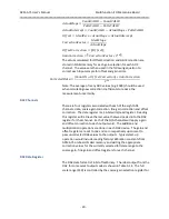
Страница 15: ... Offset Channel 8 0224 0247 Unused 0228 024B DAC Gain Channel 1 0248 024F DAC Gain Channel 2 024C 0253 DAC Gain Channel 3 0250 0267 DAC Gain Channel 8 0264 Board Status and Reset Register Read Write PCIBar2 8000H This read write register is used to issue a software reset view and clear pending interrupts and to identify the attached AXM module It may also provide other functions that are defined b...

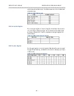
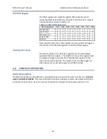
Страница 16: ...3 4 for a description of each of the register bits Table 3 4 Control Register 8100H BIT FUNCTION 31 FIFO overflow interrupt enable 30 FIFO half full interrupt enable 29 28 Amplifier Gain 00 Gain 1 full scale input range 10 24 Volts 01 Gain 2 full scale input range 5 12 Volts 10 Gain 4 full scale input range 2 56 Volts 11 Gain 8 full scale input range 1 28 Volts 27 FLASH Select This bit is connecte...

Страница 17: ...gital I O Read Write PCIBar2 810CH The Digital I O register provides access to the 16 digital I O lines Digital I O lines are pulled high via a 4 75K Ohm resistor to 5 Volts The levels of the digital I O lines are returned upon a read to this address The appropriate output enable bit must be 1 in the Digital I O Direction register to enable writing to a digital output Table 3 7 Digital I O 810CH B...

Страница 18: ...on Register Read Write PCIBar2 8118H The Digital I O Direction provides an output enable for each of the 16 digital I O lines Write a 1 to a bit to enable the output Table 3 11 Digital I O 8118CH BIT FUNCTION 31 16 unused 15 0 Digital I O Direction 15 0 0 input 1 output ADC Channels There are three registers associated with each of the sixteen ADC channels data gain correction and offset correctio...

Страница 19: ...able 3 12 ADC Data Format DESCRIPTION DIGITAL OUTPUT Full Scale FFFF Midscale zero 8000 1 LSB Below Midscale 7FFF Full Scale 0000 ADC Offset Register The offset register contains a 16 bit two s complement value that is added to the value output from the ADC to correct offset errors There is a separate offset register for each channel ADC Gain Register The gain register is a 17 bit fixed point posi...

Страница 20: ...rmance is affected by four error sources These are the instrumentation amplifier difference amplifier ADC reference and the ADC Each of these devices can contribute to the offset and gain error of the system These errors can be corrected by calibration Analog Input Channel Calibration Procedure Accurate calibration of the analog input channel digitized values can be accomplished by applying extern...

Страница 21: ...our registers associated with each of the eight ADC channels data coarse gain correction fine gain correction and offset correction The data register is a 16 bit write read register Reading this register will retrieve the last value that was loaded into the DAC register for that channel Each of the D A channels will apply a gain and offset correction to each output word The addition and multiplica...

Страница 22: ...register that allows the selection of one of three Full Scale Ranges 10 10 2564 and 10 5263 Volts as shown in Table 3 15 There is a separate coarse gain register for each channel Table 3 15 DAC Coarse Gain Selections FSR Volts Register Value 10 0 10 2564 1 10 5263 2 DAC Fine Gain Register The fine gain register is a six bit register that allows the user to adjust the gain of each DAC by 32 LSBs to...

Страница 23: ...rol register must be written to trigger a transfer from the DAC data registers to the DAC offset register Updating DAC outputs The values written to the DAC data registers are not immediately applied to the DAC outputs The LDAC bit in the control register must be written to trigger a transfer from the DAC data registers to the DAC outputs see Table 3 4 The transfer from the data register to DAC ou...

Страница 24: ...ntents of the DIG_OUT_n flip flop will be A B C D CMC BEZEL SHOWN INSTALLED AXM MODULE CHEESE HEAD SCREW M2 5 x 4 METAL STANDOFF 2 PLACES CHEESE HEAD SCREW M2 5 x 4 MEZZANINE CONNECTOR PMC CONNECTOR AXM A75 MECHANICAL ASSEMBLY WITH CMC BEZEL INSTALLED 4502 154 COMPONENT SIDE OF MODULE PMC XMC MODULE 5 TIGHTEN JACK SCREWS ITEM A 2 PLACES 1 LOOSEN JACK SCREWS ITEM A ASSEMBLY PROCEDURE COMPONENT SIDE...

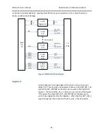
Страница 25: ...h the EDK provides access to only a single quad DAC at a time The CLR BIN2SCOMP and RESET signals are common to both DACs Analog Inputs Each of the analog input channels consists of a differential low pass filter followed by an instrumentation amplifier a difference amplifier and an ADC The differential low pass RC filter is intended to reduce RF interference The 3db cutoff frequency of the filter...

Страница 26: ...epair and service tools are used Further Acromag has automated test equipment that thoroughly checks the performance of each board Please refer to Acromag s Service Policy Bulletin or contact Acromag for complete details on how to obtain parts and repair PRELIMINARY SERVICE PROCEDURE Before beginning repair be sure that all of the procedures in section 2 0 PREPARATION FOR USE have been followed Re...

Страница 27: ...ule will work in most Acromag air cooled non processor carriers including the AcPC46xx APC PMC APCe867x VPX482x models It is not compatible with the VPX481x series or any Acromag processor board that has a PMC XMC slot Contact the factory with any questions Connectors P1 FPGA Interface 162 pin receptacle 5 mm stack height high speed terminal strip Samtec QTS 075 01 L D A K J1 Field I O 68 pin VHDC...

Страница 28: ... 60 Hz Input Channel to Input Channel Rejection Ratio1 41 dB typical 100 kHz Output Channel to Input Channel Rejection Ratio2 85 dB typical 1 kHz Accuracy Gain Full Scale 25 C Full Scale 0 70 C 1 0 011 0 026 2 0 013 0 029 4 0 015 0 033 8 0 018 0 040 Programmable Gain Instrumentation Amplifier Device ADI AD8251 PGA Linearity Error 0 005 maximum 3 27 LSB Offset Error RTI3 1 0 mV typical 2 5 mV maxim...

Страница 29: ...m C maximum Thermal Hysteresis4 100 ppm first cycle 25 ppm additional cycles Noise 78 µV RMS typical Analog to Digital Converter ADC ADI AD7686 A D Resolution 16 bits Data Format straight binary No Missing Codes no missing codes 15 bits A D Integral Linearity Error 0 6 LSB typical 2 LSB maximum Offset Error 0 1 mV typical 10 V range 1 6 mV maximum Gain Error Temperature Drift 0 3 ppm C typical Off...

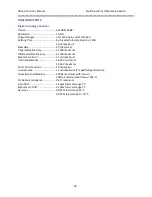
Страница 30: ...mum Slew Rate 5 V µS typical Integral Nonlinearity 2 LSB maximum Differential Nonlinearity 1 LSB maximum Bipolar Zero Error 2 mV maximum Internal Reference 4 995 V minimum 5 005 V maximum Short Circuit Current 10 mA typical Load Current 1 mA maximum for specified performance Capacitive Load Stability 200 pF maximum with RLOAD 1000 pF maximum with RLOAD 10K Ω DC Output Impedance 0 3 Ω maximum Gain ...

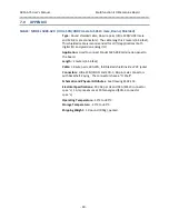
Страница 31: ...ions both digital I O and precision analog I O Application Used to connect Model 5025 288 termination panel to the board Length 2 meters 6 56 feet Cable 34 wire pairs 28 AWG foil braided shield inside a PVC jacket Connectors Ultra SCSI VHDCI and SCSI 3 68 pin male connectors with backshell Keying The connectors have a D Shell Schematic and Physical Attributes See Drawing 4502 153 Electrical Specif...

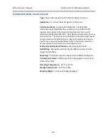
Страница 32: ...5028 432 Field signals are accessed via screw terminal strips The terminal strip markings on the termination panel 1 68 correspond to field I O pins 1 68 on the board Each board has its own unique pin assignments Refer to the board manual for correct wiring connections to the termination panel Schematic and Physical Attributes See Drawing 4501 920 Field Wiring 68 position terminal blocks with scre...

Страница 33: ...HDCI TO SCSI 3 68 PIN CABLE ASSEMBLY SHIELDED 4502 153A 4 2 6 9 2 2 5 5 8 8 37 36 3 2 1 39 38 5 42 41 8 45 44 12 11 48 47 14 13 51 50 17 16 TB1 54 53 20 19 56 55 23 22 59 58 26 25 62 61 29 28 27 65 64 31 30 68 67 34 33 ModeL Serial TB2 1 J1 3 3 6 6 7 9 9 12 12 11 11 15 15 14 14 PIN1 18 18 17 17 21 21 20 20 24 24 23 23 27 27 26 26 30 30 29 29 33 33 32 32 36 36 35 35 39 38 39 38 42 42 41 41 45 45 44...

Страница 34: ...e Clear Flash memory by erasing all sectors of the Flash Note calibration constants can be restored by repeating calibration procedure Acromag Representative Name Russ Nieves Title Dir of Sales and Marketing Email rnieves acromag com Office Phone 248 295 0838 Office Fax 248 624 9234 Revision History Release Date Version EGR DOC Description of Revision 19 FEB 13 A JCL Initial Acromag release 29 JUL...

Страница 35: ...l service in house repair center WE BUY USED EQUIPMENT Sell your excess underutilized and idle used equipment We also offer credit for buy backs and trade ins www artisantg com WeBuyEquipment REMOTE INSPECTION Remotely inspect equipment before purchasing with our interactive website at www instraview com LOOKING FOR MORE INFORMATION Visit us on the web at www artisantg com for more information on ...

Отзывы: