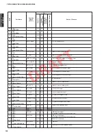
Pin
No.
Function Name
TYPE
(1)
PULL
(2)
Detail of Function
L10
VSS (Ground)
GND
–
Ground pins
M6
VSS (Ground)
GND
–
M7
VSS (Ground)
GND
–
M10
VSS (Ground)
GND
–
M11
VSS (Ground)
GND
–
T1
VSS (Ground)
GND
–
T2
VSS (Ground)
GND
–
T15
VSS (Ground)
GND
–
T16
VSS (Ground)
GND
–
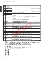
(1) I = Input, O = Output, I/O = Bidirectional, Z = High impedance, PWR = Supply voltage, GND = Ground, A = Analog signal.
Note:
The pin type shown refers to the input, output or high-impedance state of the pin function when configured as the signal name
highlighted in bold. All multiplexed signals may enter a high-impedance state when the configured function is input-only or the
configured function supports high-Z operation. All GPIO signals can be used as input or output. For multiplexed pins where
functions have different types (ie., input versus output), the table reflects the pin function direction for that particular peripheral.
(2) IPD = Internal Pull-down resistor, IPU = Internal Pull-up resistor
(3) Open drain mode for RESETOUT function.
(4) As these signals are internally pulled down while the device is in reset, it is necessary to externally pull them high with resistors if
UART1 boot mode is used.
(5) Core power supply LDO output for USB PHY. This pin must be connected via a 0.22 -uF capacitor to VSS. When the USB peripheral is
not used, the USB_VDDA12 signal should still be connected via a 1-uF capacitor to VSS.
(6) GP7[14] is initially configured as a reserved function after reset and will not be in a predictable state. This signal will only be stable after
the GPIO configuration for this pin has been completed. Users should carefully consider the system implications of this pin being in an
unknown state after reset.
98
YSP-CU4300/YSP-CU3300/NS-WSW160
Y
SP-CU430
0/Y
SP-CU330
0/
NS-WSW1
60
DRAFT


