®
ADS7807
10
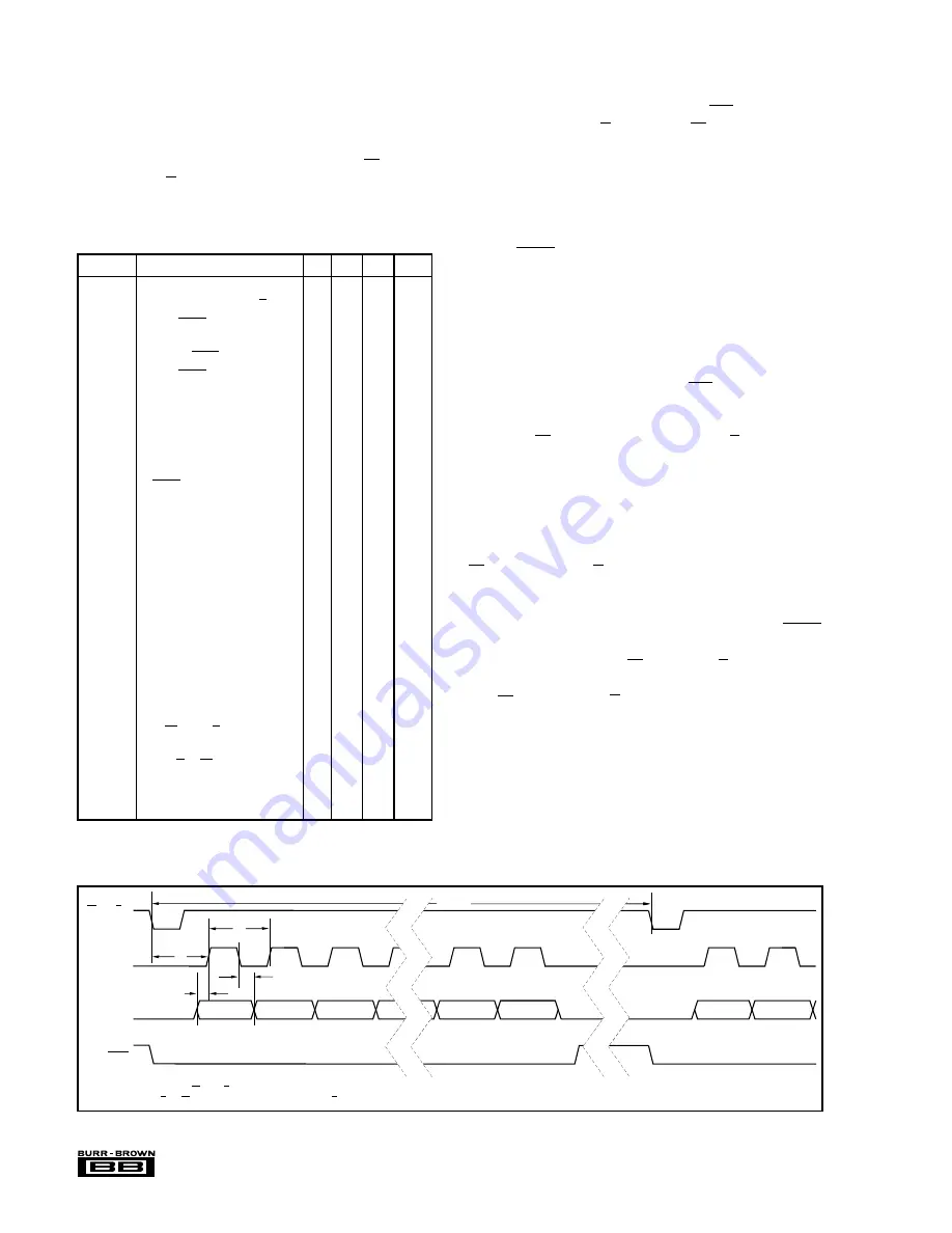
INTERNAL DATA CLOCK (During a Conversion)
To use the internal data clock, tie EXT/INT (pin 8) LOW.
The combination of R/C (pin 22) and CS (pin 23) LOW will
initiate conversion ‘n’ and activate the internal data clock
(typically 900kHz clock rate). The ADS7807 will output 16
bits of valid data, MSB first, from conversion ‘n-1’ on
SDATA (pin 19), synchronized to 16 clock pulses output on
DATACLK (pin 18). The data will be valid on both the
rising and falling edges of the internal data clock. The rising
edge of BUSY (pin 24) can be used to latch the data. After
the 16th clock pulse, DATACLK will remain LOW until the
next conversion is initiated, while SDATA will go to what-
ever logic level was input on TAG (pin 20) during the first
clock pulse. Refer to Table VI and Figure 4.
EXTERNAL DATA CLOCK
To use an external data clock, tie EXT/INT (pin 8) HIGH. The
external data clock is not a conversion clock; it can only be
used as a data clock. To enable the output mode of the
ADS7807, CS (pin 23) must be LOW and R/C (pin 22) must
be HIGH. DATACLK must be HIGH for 20% to 70% of the
total data clock period; the clock rate can be between DC and
10MHz. Serial data from conversion ‘n’ can be output on
SDATA (pin 19) after conversion ‘n’ is completed or during
conversion ‘n + 1’.
An obvious way to simplify control of the converter is to tie
CS LOW and use R/C to initiate conversions.
While this is perfectly acceptable, there is a possible prob-
lem when using an external data clock. At an indeterminate
point from 12
µ
s after the start of conversion ‘n’ until BUSY
rises, the internal logic will shift the results of conversion ‘n’
into the output register. If CS is LOW, R/C HIGH, and the
external clock is HIGH at this point, data will be lost. So,
with CS LOW, either R/C and/or DATACLK must be LOW
during this period to avoid losing valid data.
SERIAL OUTPUT
Data can be clocked out with the internal data clock or an
external data clock. When using serial output, be careful
with the parallel outputs, D7-D0 (pins 9-13 and 15-17), as
these pins will come out of Hi-Z state whenever CS (pin 23)
is LOW and R/C (pin 22) is HIGH. The serial output can not
be tri-stated and is always active. Refer to the Applications
Information section for specific serial interfaces.
FIGURE 4. Serial Data Timing Using Internal Data Clock (TAG tied LOW).
1
MSB Valid
CS or R/C
(1)
DATACLK
SDATA
BUSY
t
7
+ t
8
t
16
t
15
t
14
t
13
2
3
15
16
Bit 14 Valid
Bit 1 Valid
Bit 13 Valid
LSB Valid
NOTE: (1) If controlling with CS, tie R/C LOW. Data bus pins will remain Hi-Z at all times.
If controlling with R/C, tie CS LOW. Data bus pins will be active when R/C is HIGH, and should be left unconnected.
1
MSB Valid
2
Bit 14 Valid
(Results from previous conversion.)
SYMBOL
DESCRIPTION
MIN
TYP
MAX UNITS
t
1
Convert Pulse Width
0.04
12
µ
s
t
2
Data Valid Delay after R/C LOW
19
20
µ
s
t
3
BUSY Delay from
85
ns
Start of Conversion
t
4
BUSY LOW
19
20
µ
s
t
5
BUSY Delay after
90
ns
End of Conversion
t
6
Aperture Delay
40
ns
t
7
Conversion Time
19
20
µ
s
t
8
Acquisition Time
5
µ
s
t
9
Bus Relinquish Time
10
83
ns
t
10
BUSY Delay after Data Valid
20
60
ns
t
11
Previous Data Valid
12
19
µ
s
after Start of Conversion
t
12
Bus Access Time and BYTE Delay
83
ns
t
13
Start of Conversion
1.4
µ
s
to DATACLK Delay
t
14
DATACLK Period
1.1
µ
s
t
15
Data Valid to DATACLK
20
75
ns
HIGH Delay
t
16
Data Valid after DATACLK
400
600
ns
LOW Delay
t
17
External DATACLK Period
100
ns
t
18
External DATACLK LOW
40
ns
t
19
External DATACLK HIGH
50
ns
t
20
CS and R/C to External
25
ns
DATACLK Setup Time
t
21
R/C to CS Setup Time
10
ns
t
22
Valid Data after DATACLK HIGH
25
ns
t
7
+ t
8
Throughput Time
25
µ
s
TABLE VI. Conversion and Data Timing. T
A
= –40
°
C to
+85
°
C.


